Facebook
 Google
 GitHub
 Linkedin
Discrete Semiconductor Devices and Circuits
PN Junctions
19 questions By Tony R. Kuphaldt
-
Question 4 of 19
When “P” and “N” type semiconductor pieces are brought into close contact, free electrons from the “N” piece will rush over to fill holes in the “P” piece, creating a zone on both sides of the contact region devoid of charge carriers. What is this zone called, and what are its electrical characteristics?
Reveal answerThis is called the depletion region, and it is essentially an insulator at room temperatures.
Notes:Students should know that both “N” and “P” type semiconductors are electrically conductive. So, when a depletion region forms in the contact zone between two differing semiconductor types, the conductivity from end-to-end must be affected. Ask your students what this effect is, and what factors may influence it.
-
Question 5 of 19
What happens to the thickness of the depletion region in a PN junction when an external voltage is applied to it?
Reveal answerThe answer to this question depends entirely on the polarity of the applied voltage! One polarity tends to expand the depletion region, while the opposite polarity tends to compress it. I’ll let you determine which polarity performs which action, based on your research.
Notes:Ask your students what effect this change in depletion layer thickness has on overall conductivity through the PN junction. Under what conditions will the conductivity be greatest, and under what conditions will the conductivity be least?
-
Question 6 of 19
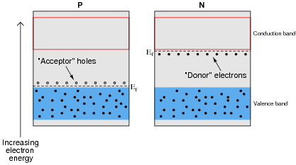
Shown here are two energy diagrams: one for a “P” type semiconducting material and another for an “N” type.
Next is an energy diagram showing the initial state when these two pieces of semiconducting material are brought into contact with each other. This is known as a flatband diagram:
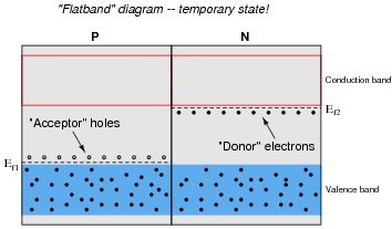
The state represented by the “flatband” diagram is most definitely a temporary one. The two different Fermi levels are incompatible with one another in the absence of an external electric field.
Draw a new energy diagram representing the final energy states after the two Fermi levels have equalized.
Note: Ef represents the Fermi energy level, and not a voltage. In physics, E always stands for energy and V for electric potential (voltage).
Reveal answer
Electrons from the N-piece rushed over to fill holes in the P-piece in order to achieve a lower energy state and equalize the two Fermi levels. This displacement of charge carriers created an electric field which accounts for the sloped energy bands in the middle region.
Follow-up question: what is this middle region called?
Notes:This is one of those concepts I just couldn’t understand when I had no comprehension of the quantum nature of electrons. In the “planetary” atomic model, there is no reason whatsoever for electrons to move from the N-piece to the P-piece unless there was an electric field pushing them in that direction. And conversely, once an electric field was created by the imbalance of electrons, the free-wheeling planetary theory would have predicted that the electrons move right back where they came from in order to neutralize the field.
Once you grasp the significance of quantized energy states, and the principle that particles do not “hold on” to unnecessary energy and therefore remain in high states when they could move down to a lower level, the concept becomes much clearer.