Facebook
 Google
 GitHub
 Linkedin
Discrete Semiconductor Devices and Circuits
PN Junctions
19 questions By Tony R. Kuphaldt
-
Question 7 of 19
Draw an energy diagram for a PN semiconductor junction under the influence of a reverse external voltage.
Reveal answer
Note: Ef represents the Fermi energy level, and not a voltage. In physics, E always stands for energy and V for electric potential (voltage).
Notes:Here it is very important that students understand the effects an electric field has on energy bands.
-
Question 8 of 19
Draw an energy diagram for a PN semiconductor junction under the influence of a forward external voltage.
Reveal answer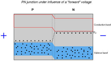
Note: Ef represents the Fermi energy level, and not a voltage. In physics, E always stands for energy and V for potential (voltage).
Notes:Here it is very important that students understand the effects an electric field has on energy bands.
-
Question 9 of 19
Draw an energy diagram for a PN semiconductor junction showing the motion of electrons and holes conducting an electric current.
Reveal answerFor the sake of clearly seeing the actions of charge carriers (mobile electrons and holes), non-moving electrons in the valence bands are not shown:

The “ ” and “-” signs show the locations of ionized acceptor and donor atoms, having taken on electric charges to create valence-band holes and conduction-band electrons, respectively.
Note: Ef represents the Fermi energy level, and not a voltage. In physics, E always stands for energy and V for potential (voltage).
Notes:Students will probably ask why there are a few holes shown in the N-type valence band, and why there are a few electrons in the P-type conduction band. Let them know that just because N-type materials are specifically designed to have conduction-band electrons does not mean they are completely devoid of valence-band holes, and visa-versa! What your students see here are minority carriers.