 Facebook
 Google
 GitHub
 Linkedin
Determining Copper Trace Thickness in PCB Design
This article discusses the issues surrounding trace-width calculation and provides a solid foundation for designing your next high-current net.
Unless you design boards with high-current nets for a living, you’ve likely never learned how to properly calculate trace-and-space width for high-current nets. There’s a good chance that you’ve visited an online calculator that determines your trace width and copper thickness for you. Unfortunately, almost all of the calculators currently online are based on outdated models. This article discusses the issues surrounding trace-width calculation and provides a solid foundation for designing your next high-current net.
Common Causes of PCB Failures
Both high-temperatures and high-temperature fluctuations can cause failures in printed circuit board components and interconnects. This section briefly details concerns surrounding high-operating-temperature and high-temperature-fluctuations in PCB design. While helpful, they are not critical to the topic at hand and you may skip ahead to “Measuring Trace Width and Copper Thickness: Past and Present” below.
High-Operating-Temperature Failures
There are a variety of component failure mechanisms, but the Arrhenius equation is generally used to predict the rate of component failure due to high operating temperature.
$$\text{A}_\text{T}=Exp \left[\frac{-E_{aa}}{k_B}\left(\frac{1}{T_1}-\frac{1}{T_2})\right) \right]$$
Equation 1. The Arrhenius equation.
Everything decomposes given enough time and thermal energy. Atoms move, molecules form new bonds, etc. The more thermal energy that enters the system, the less time required for decomposition. The Arrhenius equation can determine the acceleration factor for semiconductor time-to-failure distributions. See the resource “Reliability Derating Procedures” for example calculations. Essentially, for each increase of 15°C, failure rates of PCB components increase by a factor of 1.1 (resistors) to 2.0 (transistors).
At high enough temperatures, the PCB dielectric materials will decompose and the copper traces will vaporize. For low-grade FR-4, this dielectric decomposition happens at around 120 -130°C. That temperature is relatively easily reached by the PN junction of a power-FET, such as the TLV62065. So if you allow the thermal energy generated by an IC or trace to stay in one location on a PCB, it can melt the fiberglass and cause localized board failure.
Your PCB dielectric material properties, the expected service environment, and the service life of your design will dictate the appropriate temperature rise for your PCB.
High-Temperature Fluctuation Failures
PCBs are made of a variety of disparate materials. This is a problem in that different materials have different coefficients-of-expansion (CoE). What’s worse, many PCB dielectric materials are anisotropic, meaning the material properties are different in the x, y, and z directions.
Due to the fiberglass weave pattern in a PCB substrate, most PCBs have out-of-plane CoE that is one or two orders-of-magnitude greater in the out-of-plane direction than in the in-plane direction. The out-of-plane CoE for dielectric is several orders-of-magnitude greater than the CoE for copper. That means as temperatures rise, the dielectric materials push the board apart while the copper via barrel walls try to hold the board together. Eventually, stress cracks appear in the copper layers or via walls, breaking electrical conductivity in a net.
.gif)
Figure 1. The z-axis thermal expansion of laminate is greater than the expansion for copper. The differential stresses eventually lead to the failure of vias and copper foil. Image courtesy of PWBCorp.
In short — to have a design with a long service life, you need to both keep your PCB operating temperature low and limit the cycle frequency and temperature fluctuation of your design.
Thermodynamics Considerations
Materials with high thermal conductivity also tend to have high electrical conductivity. Of materials found on a printed circuit board, copper is second only to silver in its electrical and thermal conductivity. At \(400 \frac{W}{m \cdot K}\), copper conducts heat in a circuit board significantly better than aluminum and gold.
The PCB Base material FR-4 has a thermal conductivity that is 102 times less than copper (\(~0.4 \frac{\text{W}}{\text{m}\cdot \text{K}}\)). Therefore, if present, copper is usually the primary thermal conductor on a PCB and you are going to use copper to move thermal energy through and along your board where it will eventually dissipate via convection into the environment.
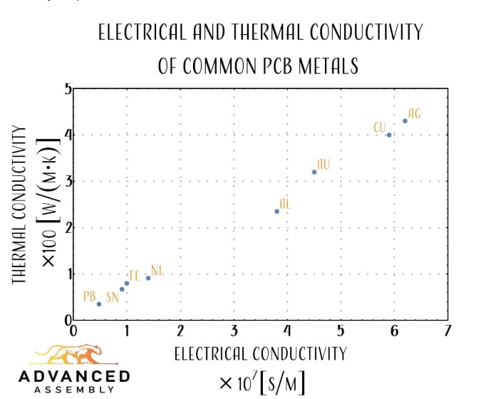
Figure 2. The electrical and thermal conductivity of metals commonly used on a PCB shows a strong correlation between thermal and electrical connectivity. At this scale, insulators would all be near the axes origin.
The current-carrying capacity of a piece of copper is determined, to a first-order approximation, by two factors — the rate of heat generation and the rate of heat dissipation. Heat is generated through ohmic heating \(\text{P}=\text{I}^2 \cdot \text{R}\) of the copper trace. Heat is dissipated through conduction, convection, and radiation. Conduction occurs across and through the PCB dielectric, convection takes place through the air, and radiation sends energy via photons into the environment. Those two broad-factors reach equilibrium points at specific temperatures for a given current and cross-sectional shape of copper.
Measuring Trace Width and Copper Thickness: Past and Present
For decades, IPC-2221 was the go-to standards document that gave engineers the trace width and copper thickness required for a given current. In 1956, two underfunded researchers created a set of experiments that generated “tentative” data that somehow survived as the de-facto standard until 2012 when IPC-2152 superseded IPC-2221. Unfortunately, many websites never got that memo — so the trace calculations most junior engineers use are based on outdated and unfounded data from 1956.
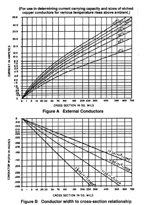
Figure 3. These graphs from IPC-2221 use outdated models from the mid-20th Century and incomplete datasets with unfounded assumptions. Extrapolated data from these graphs were used to create the online calculators you find in a cursory web search for “trace width current calculator.”
IPC-2152 uses empirically generated datasets and demonstrates that the data used to generate IPC-2221 design equations are far too conservative. In fact, the “rule” that an internal-trace must be derated by 50% can be traced back to these same researchers who didn’t research the topic due to lack-of-funding and simply made up the 50%.
In certain cases, internal traces can be derated by as little as 5%. That is because the thermal conductivity of dielectrics is marginally higher than the thermal conductivity of air — so the board-air interface is the limiting factor, not the laminate-copper interface.

Figure 4. This image from Dr. Brook’s book is taken from IPC-2152. It shows the revised calculations for PCBs.
In their book Trace Currents and Temperatures Revisited (PDF) Drs. Douglas Brooks and Johannes Adams took the data and used it to generate mathematical models for engineers to use in their designs. One such model for a copper trace in normal atmospheric conditions near the surface of the Earth is this:
$$\text{width}^{1.15}=\frac{215.3}{\triangle T}\frac{\text{current}^2}{\text{thickness}}$$
Equation 2. A mathematical model for a copper trace in normal atmospheric conditions.
You’ll notice that width is of greater physical importance than thickness — a fact that was not taken into consideration in IPC-2221. Width is measured in [mils], current is measured in [Amperes], and thickness is measured in [ounces][foot]-2.
The 215.3 is a scale factor chosen when dealing with external traces in a standard temperature and pressure environment. This number decreases for internal traces, high-altitude, and low-pressure environments.
In the article, Drs. Brooks and Adams use the graphs to generate mathematical models. While the graphs stay in the same general format as IPC-2221, they remain conceptually difficult to comprehend and master. So in preparation for a presentation at PCBWest in 2019, Advanced Assembly rearranged the equations found by Drs. Brooks and Adams to solve for different variables.
Justification for Rearranging the Equations
Equations can be rearranged in any fashion that makes them make sense to you. The way the data is presented in IPC-2221 and IPC-2152 doesn’t make much sense to me, so I looked for a simpler way to display the data.
Copper Weights Should Be the Isolines
When a designer chooses the finished copper weight from off-the-shelf copper-clad products, the quality is higher, production is faster, and the price is lower compared to requesting a custom electro-plated thickness. If you simply request “3 ounce copper” (3 oz/ft2) instead of 2 oz plated to 3 oz, you are going to get a higher-quality product for less money. Therefore, the iso-lines in the graph should likely be copper-clad thicknesses of commonly available products. That way it is easy to see the width for a given thickness and current.
Temperature Change Should Be a Constant
The allowable temperature variation should depend on the material properties of the substrate as well as the expected maximum temperature of the environment (less a margin for safety).
Assume, for example, that my design will be in a location where the ambient temperature is usually 40°C and reaches 55°C a few times a year. If my PCB dielectric manufacturer recommends I keep the temperature of the board below 85°C, I’ve got a 30°C temperature differential to work with.
It’s usually not a good idea to push the maximum operating limits, so I decided that 20°C is the maximum allowable increase in temperature. Once selected, \(\Delta T\) becomes a constant — a maximum never to be exceeded. Once that value is selected, it becomes a constant in the equation.
Use a Log-Log Plot
For most people, I believe that equations produce numbers while graphs produce understanding. If I can use the graph to get close and make basic design decisions, I can use the equations to produce desired results. The two variables that are allowed to change, width and current, are both raised to an exponent. The easiest way to straighten them out is to use a log-log plot.

Figure 5. This animation shows the relationship between trace width and current for a variety of common copper-clad thicknesses. The lines start above the horizontal axis because different thicknesses of copper have different minimum manufacturing minimums for trace-width.
Now everything is a series of nice-straight lines. As an engineer, you can take known quantities, such as the allowable temperature increase and current, and quickly find an appropriate trace-width and copper thickness. Once you have a good idea of trace-width and copper weight you can use the equations to better zero-in on your target value.
Final Thoughts and Tests
Standard disclaimers always apply—you are still responsible for your work. If your board bursts into flame, it is not sufficient to tell the legal department, “Some guy on the internet told me this would work.” I am definitely not telling you that. I am telling you this will get you very close. At that point, you should simulate your design in a multi-physics simulator that perhaps includes computational fluid dynamics.
Then you should test your board in real-world conditions and track the temperature with a thermal-camera.
Additional Resources
“Fabricating Heavy Copper PCBs for High Current Applications” by Greg Ziraldo, Senior Director of Operations at Advanced Assembly. This webinar is identical to the presentation given at PCBWest in 2019.
Elijah Gracia and Jon Lass, Engineers at Royal Circuit Solutions provided the fabrication minimums used in these graphics and can provide answers to specific fabrication questions related to any design.
Figure 6 shows the preferred manufacturing minimum trace/space widths at Royal Circuit Solutions for a variety of copper weights. Exceeding these limits is possible, but excursions will adversely affect the overall per-panel yield. Minimums vary by manufacturer and by technology.
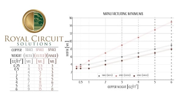
Figure 6. The preferred manufacturing minimum trace/space widths at Royal Circuit Solutions for a variety of copper weights.
Related Content


Just a note: I made some additional graphs at the request of RoyalCircuits.com for their website. If you need other temperatures, see https://www.royalcircuits.com/space-trace-appendix/
Also, remember that increased operating temperature will derate your passives and affect your digital and analog ICs. So unless you’re doing downhole drilling, maybe stay away from the upper end of the scales.