Facebook
 Google
 GitHub
 Linkedin
How to Tackle Electrical Over-Stress (EOS) Challenges in the USB-PD Era
As USB PD 3.1 devices proliferate, high-voltages increase the risk of electrostatic issues. To address these problems, learn how to make smart choices in ESD and EOS testing, as well as TVS device selection.
Ever since its roll out by the USB Implementers Forum (USB-IF), the USB PD 3.1 protocol has been designed into consumer electronics, such as laptops, wearable devices, tablets, and smartphones.
In the part of the spec concerning the power delivery capability, the standard power range is defined with the maximum charging power remaining at 100 W, but with three voltage levels added to the extended power range: 28 V, 36 V, and 48 V. The corresponding current is 5 A for all three voltages, thus increasing the maximum output power from 100 W to 240 W, as shown in Figure 1.
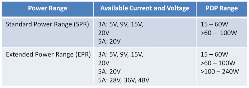
Figure 1. Fixed voltage power ranges
USB PD3.1 is centered around the physical port of USB Type C. The protocol not only only improves the transmission rate by up to 120 Gbit/s, but also supports efficient fast charging with the maximum power supply of 240 W.
Cell Phone Designs Lead the Way
For its part, the cell phone is the first application of fast charging. Among the mainstream fast charging technologies are QC charger, USB-PD, and those developed by the phone manufacturers—such as H-brand Supercharge, V-brand dual-engine, and O-brand SuperVOOC. These technologies work by increasing the charging voltage or current to boost the charging power, thus accomplishing fast charging.
The O-brand SuperVOOC works by exploiting low voltage and large current as well as the new voltage charging algorithm, a direct charging method that achieves constant voltage and current control dynamically at the adapter. In the large current charging mode, the charger charges the battery directly through the direct charging switch. The dual cells are in series for greater charging voltage.
The open-voltage loop realizes the output constant current in stages. The “open voltage loop” is a device designed based on the principle of negative feedback and its main function is to control the voltage and current during battery charging. As the charging current exceeds the predefined threshold, the open-voltage loop opens the switch in the circuit automatically to reduce the battery voltage while maintaining constant charging current.
The charging method achieves constant-current output in stages. It is effective in improving charging efficiency and safety and, therefore, the charging power at the end up to 125 W (20 V / 7.5 A). Figure 2 illustrates the principle behind the O-brand SuperVOOC.
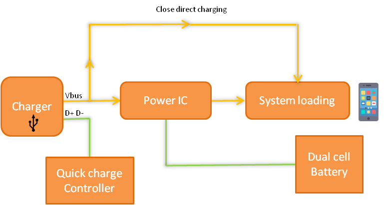
Figure 2. Fast charging principle behind O-brand SuperVOOC
Regardless of which fast charging technology is used, the power is increasing constantly. The output voltage of this charging is increasing from 5 V to 9 V / 10 V / 12 V, and it is expected to see 48 V in the future. Given that power IC designs are leveraging advanced manufacturing processes, the ICs become more vulnerable to electrical over-stress (EOS).
Electrical Over-Stress (EOS) Risk on the Rise
Today’s electronic products have become a part of our daily life and used very frequently. As a result, the demand for frequent charging keeps growing. That means that charging cables are plugged and unplugged very often, which increases the risk of EOS.
In charger cables, electrostatic discharge (ESD) discharging is the EOS damage caused by plugging and unplugging a live cable. The common source of this is the overshoot or undershoot caused by plugging and unplugging. It can be observed as the spark we see at the port when two poorly grounded systems are connected with a cable.
Meanwhile, the signal cable and power cable may be live during live plugging and unplugging. Discharging occurs when a live cable makes contact with the system. Whether this event is electrostatic discharging or direct discharging in general, it can do serious harm to the system.
ESD Testing and Direct-Pin Injection EOS Tests
For ESD testing on a system, an increasingly popular method these days is to use direct-pin injection. This simulates the ESD events that happen to the system when it is operated by the user. Beyond ESD testing, these products are very likely to be subject to EOS due to poor infrastructure in remote areas. This results in an increase in the percentage of products returned for repair.
Today, most EOS tests are performed according to IEC 61000-4-5, with a test voltage waveform of 1.2/ 50 µs and current waveform of 8 / 20 µs. Some companies request additional EOS tests using direct-pin injection. Figure 3 provides an example of a direct-pin injection EOS test setup.
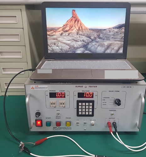
Figure 3. EOS test with direct-pin injection
Selecting the Right TVS Device
It’s important to select an appropriate transient voltage suppression (TVS) protection device for better ESD/EOS protection of electronic systems. To select the right TVS protection device, it is necessary to consider the IPP (peak pulse current) capability of the device itself against ESD/EOS.
Also, the operating voltage of the TVS device has to be as close to the PD voltage as possible. For example, a TVS device with an operating voltage of 9 V is chosen for a PD voltage of 9 V , and the same applies to a PD voltage of 15 V or 24 V.
Power Delivery works by charging with DC. With that in mind, better protection can be achieved by incorporating a unidirectional TVS device in a DC power supply. On top of that, the 0201 packaging is recommended for the TVS, since electronic products are becoming increasingly miniaturized.
For effective protection inside of a system, it’s important to consider a low clamping voltage for ESD/EOS. A low clamping voltage prevents ESD/EOS surges from entering the system and causing all kinds of troubles to the circuits. That’s why the ESD/EOS clamping voltage is an important parameter in a TVS device to ensure system circuit protection.
ESD/EOS Protection More Important Than Ever
In summary, it’s clear that, for fast charging in cell phones, EOS protection is imperative. The device’s charging port is constantly subject to EOS surge interference. Without an effective ESD/EOS protection solution at the charging port, the downstream ICs are vulnerable and the risk of product malfunction increases exponentially.
Electronic products are seen everywhere in our daily life. They are becoming smaller and smaller thanks to the introduction of advanced semiconductor manufacturing processes. In turn, TVS devices are increasingly important for these products.
With all that in mind, it is vital to include an appropriate TVS protection device at the charging port for all electronic products that are subject to frequent plugging and unplugging. One with 0201 unidirectional packaging and IPP (> 5A) is recommended for better EOS protection and so is the direct-pin injection EOS test to ensure the products’ resistance to EOS.
All images used courtesy of Amazing Microelectronic Corp. (AMC)
Related Content