Facebook
 Google
 GitHub
 Linkedin
An Introduction to SweRV, a RISC-V Core
This article introduces the RISC-V-based SweRV core, which builds on the classic five-stage RISC-V pipeline and allows up to two instructions per clock cycle.
This article introduces the RISC-V-based SweRV core, which builds on the classic five-stage RISC-V pipeline and allows up to two instructions per clock cycle.
Since the RISC-V instruction set architecture was unveiled (2015) and RISC-V foundation established (2016), we have seen a flurry of activity: many open source hardware projects, many corporate adoptions of the architecture, fast-growing membership of the foundation, and fast-growing open-source RISC-V software activity.
At the “Core” of all these projects are RISC-V CPU (Central Processing Unit) cores — hardware engines that are executing RISC-V compiler binaries. All community stakeholders benefit from the open-source software, including common compilers, toolchains, and operating systems that can execute on top of these cores.
Some of the RISC-V cores developed are proprietary (or available for IP licensing), but even more are available in the open-source domain. The availability of open-source RISC-V cores enables a large number of fully open-source hardware projects, including educational purposes and unprecedented hardware level collaboration and innovations, which otherwise would not be possible.
Open-Source RISC-V Cores
What does open source RISC-V core mean? What does “open” mean in the context of the IP cores for ASICs?
ASIC stands for application-specific integrated circuit. It is a “chip” that has a specific purpose, such as a microcontroller in a refrigerator, microwave, or hard disk drive. IP core refers to the intellectual property core and indicates a circuit that is typically a black box available for licensing, but the interfaces to this IP are known and described.
In the past, CPU cores were typically either available for licensing or open-source. Those that were available in open-source came from a variety of universities and research institutions and never had standardized instruction sets. This meant that compilers and other software tools were either unavailable or of low quality, due to never having a shared software project.
The standardization of RISC-V enabled not only sharing the software toolchain, but it also enabled sharing of the cores themselves and improving upon available open-source designs. The cores are typically designed using hardware description languages such as Verilog, System Verilog, or VHDL, or synthesized from the high-level synthesis languages such as Chisel. In any case, it is this code that is available as open source, typically under BSD or Apache v2 license.
SweRV Cores
SweRV™ cores fill an important void in the spectrum of open-source RISC-V cores (See Figure 1). For embedded applications, single-threaded code execution is quite important, as there are many legacy firmware implementations implemented as a single thread, and in some cases RTOS and multi-threading may not be practical, or simply too expensive. In those cases, cores that can run a single thread at the highest possible performance become quite important.

Figure 1. Open source RISC-V cores. Note that this graph is not exhaustive and many open-source cores are not shown.
So, how is SweRV core different? It issues up to two instructions per clock cycle, and a nine-stage pipeline with four execution units, a load/store unit, a two-cycle multiplier, and out-of-pipe 34-cycle divider units. Figure 2 shows an architecture block diagram of the classical five-stage RISC pipeline (shown in Figure 2a) and SweRV core (shown in Figure 2b).
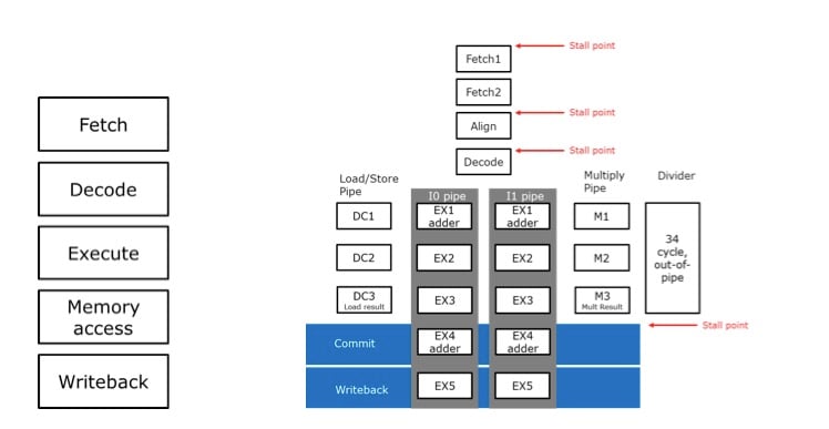
Figure 2. Block diagram comparison of a) classic 5-stage RISC-V pipeline and b) SweRV core.
Most open-sourced RISC-V designs (at least design that we are familiar with from RISC-V conferences and events) are implemented as single-issue pipelines (with a number of stages between two and six). Single-issue pipeline means that one instruction is being processed in every clock cycle. In principle, every instruction needs to be fetched (Fetch) from the memory, decoded (Decode) to figure out if it is an arithmetic instruction, such as ADD for addition, or LD for loading a register from the memory, and then it needs to be executed (Execute).
Upon execution, memory may be accessed to save the results or load registers (Memory access) and finally, results must be written back to registers (Writeback). This five-stage design is efficient and has been the basis for some commercial processors, such as early MIPS, SPARC and Motorola 88000 designs. It is still very relevant today, and many multi-core systems targeted for machine-learning workloads are using exactly this design (with an addition of wide vector Arithmetic Logic Unit). If your workload can be multi-threaded, this type of core may provide a nice balance between power, area, and performance. But what happens if you want to run legacy firmware application, and you just want to run it faster? A single program cannot run on two cores – only one. So, the solution is to try to run this core faster.
Accelerating the Pipeline
There are two ways on how the classical pipeline can be accelerated.
First, introducing more stages into the pipeline can lead to a better balance between the time durations for each stage. This allows for smaller time increments per each stage, which implies that design can be run on a higher frequency. High-end CPU cores found in powerful Intel or IBM processors may have a large number of stages, sometimes between 20 and 30. A quick inspection of Figure 2b shows that we have two Fetch stages, two Align/Decode stages, and 4 execute stages.
Second, SweRV design is superscalar – we have implemented two pipelines, I0 and I1, that can execute up to two instructions per clock cycle. Not only can we run faster (due to a large number of stages), but we can also (depending on the workload) execute 2 instructions in each clock cycle. Finally, each pipeline has arithmetic logic units in stages EX1 and EX4, which may seem unusual at first sight.
Classic pipelines (Figure 2a) suffer from an issue called “load-to-use latency”. Namely, if the register value needs to be loaded from memory (let’s think of instruction ld x11,8(x10), for all of you RISC-V assembly geeks), the latency may be long, depending on the memory hierarchy. The pipeline may be stalled for a long time. In the case of SweRV, we get a second chance at stage EX4 – so, as long as memory latency is less than 3 clock cycles, the pipeline can keep running! This feature does come at a small penalty of having dual execution units per pipeline. Finally, the load/store operations are implemented in the pipeline I0, and can be executed concurrently with the pipeline I1, unlike with the classical pipeline.
So – what is the net result? We have measured Coremark benchmark performance both on the cycle-accurate simulation of our design, and on the FPGA implementation. The results are shown in Figure 3.

Figure 3. Coremark performance benchmark, renormalized per single execution thread.
We can see that SweRV delivers about 4.9 Coremark/MHz score (score is renormalized per frequency and per single thread – that explains why it is so close to Intel Xeon core, which is a very high-performance core). This is an excellent result – something to be proud about – and something very useful for the open-source RISC-V community.
We hope that this article introduces SweRV core and its goals – both for Western Digital and the open-source hardware community. SweRV is not the end – it is just the beginning of our story of bringing one billion RISC-V cores to the marketplace.
Related Content