
Resolving the Signal: Introduction to Noise in Delta-Sigma ADCs Part 3
This 12-part article series focuses on the impact of noise in delta-sigma ADCs. Part 3 brings the theoretical information provided in parts 1 and 2 to a real-world design example.
This 12-part article series focuses on the impact of noise in delta-sigma ADCs. Part 3 brings the theoretical information provided in parts 1 and 2 to a real-world design example.
In both part 1 and part 2 of this series, I explored analog-to-digital converter (ADC) noise performance in detail, from its characteristics and sources to how it’s measured and specified. In part 3 of this series, I’ll apply the theoretical understanding from parts 1 and 2 to a real-world design example. Ultimately, the goal is to give you the knowledge necessary to answer the question, “What noise performance do I really need?” allowing you to easily and confidently choose an ADC for your next application.
System Specifications
I’ll begin the example by defining system specifications for the application, converting these specifications into a target noise-performance parameter and using that information to compare potential ADCs. As an example, let’s analyze a weigh-scale application that uses a four-wire resistive bridge similar to that shown in Figure 1.
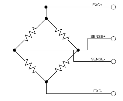
Figure 1. Typical four-wire resistive bridge
For the system specifications, assume a bridge with a sensitivity of 2mV/V and an excitation voltage of 2.5V that you want to sample at 5 samples per second (SPS). This provides a maximum output voltage of 5mV that corresponds to a maximum applied weight of 1kg. Let’s also assume that you want to be able to resolve a minimum applied weight of 50mg. Table 1 summarizes these parameters.
Now that you have the system specifications, let’s convert them into common noise parameters to help choose the best ADC.
Defining a System Noise Parameter
In part 2 of this series, I strongly recommended using input-referred noise to define system noise parameters and choose an ADC. But let’s begin with the more common approach of using noise-free counts and noise-free resolution. Then you can compare this method to using input-referred noise directly. Equations 1 and 2 calculate your initial noise parameters:

Equation 1

Equation 2
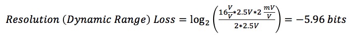
With a required noise-free resolution of 14.3 bits, you might quickly conclude that you only need a 16-bit ADC. However, as I explained in part 2, the noise-free resolution a high-resolution delta-sigma ADC can actually provide depends on the percentage utilization of the ADC’s full-scale range. In this example, the system uses a 2.5V reference voltage and the maximum input signal is the product of the excitation voltage (2.5V) and bridge sensitivity (2mV/V). Equation 3 shows the expected resolution loss using Equation 2 from part 2:
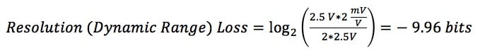
Equation 3
This is a dramatic result. Since you’re only using 0.1% of the available full-scale range, you’ll lose almost 10 bits of resolution. At this level, even a 24-bit ADC would not be sufficient to meet the system requirements. To remedy the issue, you’d need to increase the percentage utilization by either changing the system specs or amplifying the input signal. Assuming that you have little control over what the system requires, you’re left with gaining up the input, an action that absolutely changes the noise performance of the signal chain.
Fortunately, you can continue your analysis without needing a detailed understanding of how amplifier noise affects system performance. Instead, you can use your existing knowledge to analyze the data-sheet noise tables of an ADC with an integrated programmable gain amplifier (PGA) to determine if it meets the system requirements.
For example, Figure 2 shows the effective and noise-free resolution tables for the 24-bit ADS124S08 up to 50SPS, with the target data rate highlighted. Note that the ADS124S08 includes gains from 1V/V up to 128V/V.
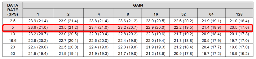
Figure 2. ADS124S08 effective resolution (noise-free resolution) – Sinc3 filter at AVDD = 3.3V, AVSS = 0V, PGA enabled, global chop disabled and internal 2.5V reference
To determine if this ADC meets your requirements, you need to recalculate the expected resolution loss for each gain setting separately, as each results in a different percentage utilization. You then need to add this to each corresponding noise-free resolution value reported in Figure 2 to see if it meets the system specifications. Table 2 lists the calculated system noise-free resolution in bits using the ADS124S08 at a 5SPS data rate.
Table 2 tells you that you can only achieve the required system noise-free resolution of 14.3 bits using a gain of 32, 64 or 128V/V at 5SPS. Figure 3 highlights these values in the context of the data-sheet noise tables.
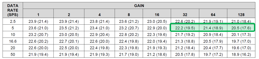
Figure 3. Gain settings that meet the system requirements using the ADS124S08 at a 5SPS data rate
One key takeaway from Figure 3 is that there is no simple way to correlate the values in the data sheet to the system-noise parameter without multiple calculations. While this may not be relevant now after calculating the results, what if the system specifications suddenly changed?
Suppose you decided to increase the excitation (reference) voltage from 2.5V to 5V. You’re also going to increase the bridge sensitivity to 20mV/V (which means that you cannot use the highest gain settings since this will over-range the ADC). And you’re exploring the option of sampling at 20SPS instead of 5SPS. How do these changes affect your ADC noise analysis?
To determine the answer, you would have to calculate a new resolution loss for each gain setting at the new data rate and reference voltage. Additionally, you would have to recreate the table in Figure 2 based off of a 5V reference voltage, since this table’s calculations use a reference voltage of 2.5V. Finally, you would have to recreate Table 2 by subtracting the calculated resolution losses from the noise-free resolution table that was created using a 5V reference voltage.
Admittedly, this is a lot of work, and is a direct result of noise-free resolution being a relative parameter. So let’s now switch to using an absolute noise parameter, as suggested in part 2, and see how the analysis changes.
Using Input-Referred Noise
Like noise-free resolution, you only need to know a few of your system specifications to determine the required input-referred noise for your bridge. You need to know its maximum output signal, which is 5mV. You also need to know the weight to which this maximum signal corresponds, which is 1kg. And finally, you need to know your minimum applied weight, which is 50mg. With these few bits of information, you can use Equation 4 to determine that your ADC needs to be able to resolve a peak-to-peak signal of 250nV:
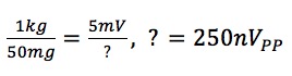
Equation 4
One of the benefits of using input-referred noise is that you don’t have to worry about calculating resolution loss. Instead, you can directly compare your calculated value against the input-referred noise table for your ADC to determine which combination of settings offers an equal or lower level of noise performance.
Figure 4 is an abridged version of the input-referred noise table for the ADS124S08. I’ve highlighted any combination of gain and data-rate settings that provides ≤250nVPP of input-referred noise.
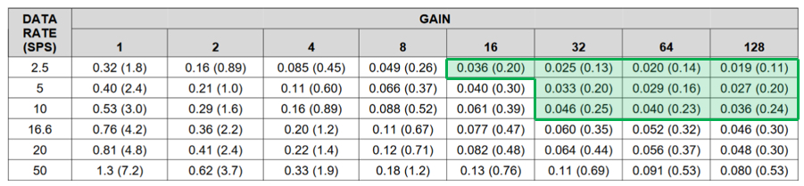
Figure 4. Data-rate and gain combinations providing ≤250nVPP using the ADS124S08 (Note: Table values are given as “noise µVRMS (µVPP)” using a 2.5V reference voltage)
If you compare the results in Figure 4 to your analysis using noise-free resolution in Figure 3, you’ll see that Figure 4 provides the entire range of ADS124S08 settings that meet the system requirements. Figure 3 only provides the values at the data rate selected and requires that you perform new calculations for different data rates, making this approach less adaptable to system specification changes.
Effects of System Changes
Let’s now assume that you’ve increased your maximum applied weight to 5kg, your minimum applied weight to 500mg and kept your bridge’s maximum output signal at 5mV, as in Equation 5:
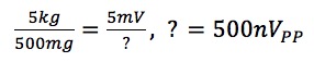
Equation 5
With a quick calculation, you can determine that your system noise requirement has been relaxed to 500nVPP, which makes more data-rate and gain combinations available to you. Figure 5 demonstrates that these relaxed system specifications allow you to sample faster (up to 20SPS) or decrease your gain (down to 4V/V) while still achieving the requisite noise performance.
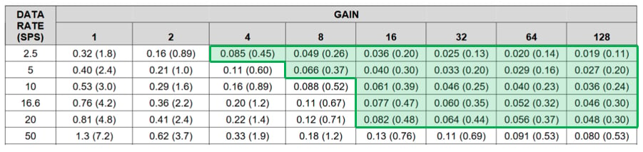
Figure 5. Data-rate and gain combinations providing ≤500nVPP using the ADS124S08 (Note: Table values are given as “noise µVRMS (µVPP)” using a 2.5V reference voltage)
What if your weigh scale requires more resolution instead? For example, you keep the 5kg maximum applied weight requirement but return to the 50mg minimum weight from the first example. Keeping your maximum bridge output the same (5mV), you now require 50nVPP of input-referred noise, which is extremely low. Looking at Figures 4 or 5, it’s clear that no combination of ADS124S08 data-rate and gain settings provide this level of performance. But because you can easily perform this same analysis with any ADC, simply choose one with better noise performance.
Figure 6 shows the noise table for the ADS1262, a 32-bit ADC that is functionally similar to the ADS124S08 but offers better noise performance. The green shading indicates the data-rate and noise combinations that provide ≤50nVPP of input-referred noise, and confirm that the ADS1262 can meet your system’s new resolution requirements.
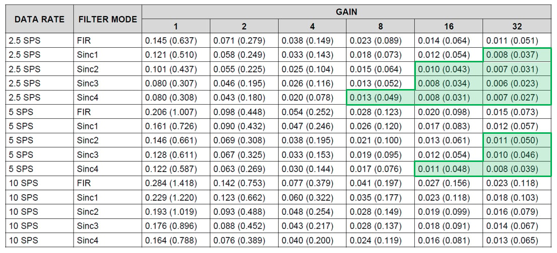
Figure 6. Data-rate and gain combinations providing ≤50nVPP using the ADS1262 (Note: Table values are given as “noise µVRMS (µVPP)” using a 2.5V reference voltage)
For the sake of argument, let’s compare the input-referred noise result to a relative parameter. Figure 7 highlights the ADS1262’s noise-free resolution performance at the same data-rate and gain configurations shown in Figure 6.
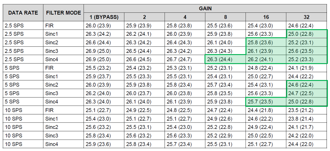
Figure 7. Effective (noise-free) resolution correlating to ≤50nVPP using the AD12626 and a 5V reference voltage
In part 2, I pointed out that many engineers were needlessly concerned with maximizing their noise-free resolution (dynamic range). Let’s examine this point by calculating your system’s noise-free resolution from the largest highlighted value at the system-required 5SPS data rate. In Figure 7, this value is 23.5 bits and is available at a gain of 16V/V using the Sinc4 filter.
Remember from Figure 7’s caption that the table calculations use a 5V reference voltage, not the 2.5V reference voltage the system specifies. To compensate for this difference, each of the resolution values given in Figure 6 must be decreased by one bit. This means that you can only expect a maximum of 22.5 bits of noise-free resolution at the given conditions. You can now calculate the expected resolution loss for the ADS1262 at these settings.
Using the result from Equation 6, the system noise-free resolution is only 16.5 bits using a 32-bit ADC.
Equation 6
For many, this is a disheartening result that seems to confirm the fear that you are paying for performance the ADC cannot actually provide. However, if you look at the same settings from Figure 6, you’ll see that you’re actually taking advantage of 48nVPP noise at the given conditions. This is an incredibly small value, which no 16-bit ADC and very few 24-bit ADCs can provide.
Ultimately, this is the point I’m trying to make. You need such a high-resolution ADC to achieve 16.5 bits of noise-free resolution (dynamic range) because the system requires extremely low noise performance. That is why it makes sense to define system performance and choose ADCs using input-referred noise.
In the next installment of the “Resolving the Signal” series, I’ll discuss effective noise bandwidth in detail and delve into topics including how to determine the amount of noise that passes into the system and methods to restrict noise bandwidth.
Industry Articles are a form of content that allows industry partners to share useful news, messages, and technology with All About Circuits readers in a way editorial content is not well suited to. All Industry Articles are subject to strict editorial guidelines with the intention of offering readers useful news, technical expertise, or stories. The viewpoints and opinions expressed in Industry Articles are those of the partner and not necessarily those of All About Circuits or its writers.


Hi Bryan. I have been going through your article regarding noise in Delta-Sigma. I have a couple of questions. When you are choosing the ADC, you recommed to use the input referred noise as an absolute parameter for selecting the right ADC, rather than effective resolution. However, you always conside the peak to peak noise voltage in your calculations. I am reviewing a design that is using the ADS1256 (24 bit, 8 channel) ADC from TI. However, the datasheet does not give any P-P noise computation, but only RMS noise. I understand that there is no relationship between the two. So, how can the same be used for choosing the ADC? Can you share some options? Also, another question pertains to the grounding of the ADC. There are diverse recommendations regarding the ADC grounding with the system grounding. While most speak about isolating the Analog Ground Plane from the Digital Ground plan, at some point these planes have to integrate into a common system ground. Therefore, how should this ground plane be connected? are there any good ways of doing it to preserve the Analog inputs from digital noise?