Facebook
 Google
 GitHub
 Linkedin
ROHM’s High Voltage GaN Solutions With EcoGaN
Gallium nitride (GaN) power solutions have a strong foothold in medium-powered applications including consumer electronics, EV onboard chargers (OBCs), and DC/DC converters.
GaN’s high-electron-mobility transistor’s (HEMT’s) high power figure of merit (FoM), allows the wideband gap (WBG) semiconductor to operate at high frequencies and withstand high powers while successfully dissipating all this energy. This advantage can support the semiconductor technology to be groundbreaking not only in its power handling, but also in its efficiency.

Image used courtesy of Adobe Stock
However, there are design hurdles that can prevent designers from taking advantage of the strengths of this substrate. GaN HEMTs are notoriously problematic when it comes to driving its gate, and there is a small margin for error with mistakes that can lead to other, more significant failures.
ROHM has an established expertise in GaN development starting with their 150 V GaN HEMT in 2022, developed after 20 years of research. Since then, ROHM has steadily improved and maintained a high quality that is essential for growing GaN epilayers for GaN-on-Si technology. The newest introduction into the EcoGaN lineup is the 650 V GaN Power Stage, integrating a gate driver and the analog-based GaN driving IC for a tightly controlled GaN HEMT, which does not suffer from the common downsides of this technology. This technical article describes the EcoGaN 650 V Power Stage IC and its benefits within various power applications.
The Growing Benefits of GaN as a Power Device
A Brief History
WBG semiconductors such as GaN and silicon carbide (SiC) have steadily permeated power device applications from consumer appliances and battery electric vehicles (BEVs) to base station amplifiers for next-generation wireless systems and traction inverters in electric railways. Initially, GaN found traction in LED lighting applications due to its ability to emit a wide range of wavelengths in the visible spectrum. GaN laser diodes (LDs) were also realized due to GaN’s inherently good high frequency characteristics, making it a contender with other III-V compound semiconductors found in photonics such as gallium arsenide (GaAs) and indium phosphide (InP). These characteristics made GaN a growing option for high power microwave and millimeter-wave applications, such as high power amplifiers (HPAs) for base stations, rapidly replacing conventional Si LDMOS alternatives. GaN also became an option in military applications within phased array antennas. The power handling of GaN—with its high energy gap, good thermal conductivity, and high breakdown electric field—made this substrate penetrate the power device market often beginning with consumer electronics devices such as GaN-based adapters and chargers.

Figure 1. GaN properties and advantages. Image used courtesy of ROHM Semiconductor
GaN and SiC Power Devices
GaN has become a strong option for medium-range power devices alongside SiC. Both materials have: high power handling capabilities, reducing the size of the transistor and simplifying thermal management of the die; high switching frequencies, reducing both the size of external passive components and the burden on filtering components; potentially high device efficiency with the channel resistance (Rds(on)) and gate charge (Qg) optimized for lower conduction and switching losses. While SiC currently dominates the higher parts of the power spectrum, with 750 V and 1200 V transistors commonly occurring, GaN devices will generally max out at around 650 V. Figure 2 shows the switching power versus operating frequencies of various high-power applications and the existing technologies that generally support them including Si insulated-gate bipolar transistors (IGBTs), Si super junction (SJ) MOSFETs, SiC, and GaN.
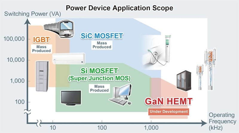
Figure 2. The switching power and operating frequency offered by various power devices technologies as well as common applications within this power spectrum. Image used courtesy of ROHM Semiconductor
There are strengths and drawbacks to GaN and SiC technologies. Table 2 shows the power, voltage, and frequency range of GaN and SiC technologies as well as some of the common applications these semiconductors are deployed in. GaN’s relatively convenient manufacturability is one massive benefit of this substrate. However, the high energy conversion efficiency and subsequent miniaturization of power solutions cannot truly be taken advantage of when there are any delays in driving the IC that controls the GaN power device.
Table 2. GaN and SiC characteristics and applications.
|
|
GaN |
SiC |
|
Power |
Medium-powered applications |
High-powered applications |
|
Voltage |
100 to 650 V |
< 650 V |
|
Frequency |
< 200 kHz |
20 to 200 kHz |
|
Applications |
|
|
GaN Design Challenges
GaN HEMTs have the advantage of an inherently low parasitic capacitance, yielding a high efficiency, high switching speeds, and high power density. However, this is a difficult quality to take advantage of given how “temperamental” driving the gates of these transistors are. GaN HEMTs are difficult to drive, when there is a small difference between the rated gate-source voltage (VGS) and gate driving voltage due to their device structure, leading to relatively small gate driving voltage margins. For instance, the typical VGS of an enhancement mode (E-mode) HEMT is generally 6 V, while the gate driving voltage is 5 V, leading to a driving voltage margin of 1 V. Moreover, this VGS rating cannot be exceeded without causing component degradation and possible destruction, making it paramount that the gate driving voltage never exceeds the rated VGS. This has caused vendors to create specialized gate driver ICs that can tightly control the gate drive amplitude and waveshape and restrict di/dt and dv/dt as any ringing or voltage overshoots can cause HEMT to essentially blow up. There is also a trade-off between voltage overshoot and turn-on time at the gate for these FETs, so finding a gate drive IC that can successfully maintain a fast turn-on response without causing unwanted, risky voltage overshoots is a task.
The threshold voltage (Vth) of E-mode GaN HEMTs is also quite low (0.9 to 1.5 V), further restricting the maximum dV/dt where any ringing can cause unwanted self turn-on. Generally, a large gate resistance (RG) is used to dampen any ringing at the gate however this will directly lead to switching losses and an increased turn-on time.
ROHM 650 V GaN Power Stage = GaN HEMT + Gate Driver
As shown in Figure 3, ROHM developed 650 V enhancement mode (E-mode) GaN HEMT technology that integrates a gate driver as well as several peripherals, greatly simplifying these issues. ROHM has an established expertise in integrating analog technologies, allowing the company to naturally expand their GaN product portfolio with analog control ICs, i.e., gate driver.
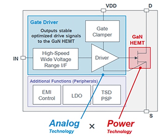
Image used courtesy of ROHM Semiconductor
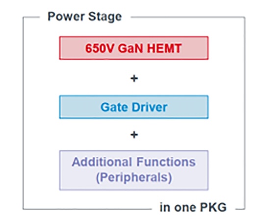
Figure 3. Block diagram of the BM3G0xxMUV-LB series with an integrated gate driver and peripherals. Image used courtesy of ROHM Semiconductor
Rohm has created an entire power stage system-in-package (SiP) with a wide driving voltage range from 2.5 to 30 V, with a ~15 µs startup time, and an 11 to 15 ns propagation delay (Figure 4). This is based upon the BM3G015MUV-LB and BM3G007MUV-LB GaN HEMT products, each with an Rds(on) of 150 mΩ and 70 mΩ.
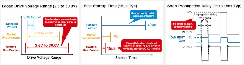
Figure 4. The new ROHM power stage lineup includes a broad drive voltage range and a fast startup time that minimizes voltage overshoots. Image used courtesy of ROHM Semiconductor
The 650 V GaN Power Stage also sidesteps the disadvantage of the low Vth that could lead to unwanted turn-ons: an extremely low gate loop inductance eliminates the risk of self turn-on up to 150 V/ns—the adjustable turn-on slew rate of this system is specified from 20 to 100 V/ns. Moreover, the zero common source inductance ensures the SiP exhibits higher switching speeds than discrete GaN HEMTs.
Another important factor to consider when using an external gate driver is the downside of additional parasitic inductance in the overall solution, leading to more switching losses and ringing. The integrated 650 V Power Stage package removes this issue for a more streamlined design.
Part and Cost Reduction
Alternative solutions with integrated gate drivers will still require many additional components to successfully embed it within a power solution. As shown in Figure 5, competitive solutions will either have a narrow VDD and VIN range as well as the need for more expensive passives while the ROHM solution requires a single capacitor and controller. This reduction in part count drops the BOM costs and simplifies overall implementation.
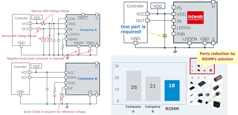
Figure 5. Alternative GaN HEMT technologies with integrated gate drivers will still require many additional passive components. Image used courtesy of ROHM Semiconductor
Application Circuits
An application circuit for the 650 V Power Stage system can be seen in Figure 6. The SiP can be easily arranged in a flyback, interleaved power factor correction (PFC), half-bridge, or totem-pole PFC configuration.
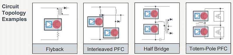
Figure 6. Potential circuit topologies of the 650 V GaN Power Stage SiP for easy integration within many power systems spanning from consumer electronics applications to EVs. Image used courtesy of ROHM Semiconductor
Another more detailed application circuit can be found in Figure 7 with a boundary conduction mode (BCM) PFC converter.

Figure 7. BCM PFC converter application circuit with the 650 V Power Stage SiP. Image used courtesy of ROHM Semiconductor
A 400 V, 240 W BM3G007MUV-EVK-002 PFC evaluation board is also available with a built in BM3G007MUV 650 V GaN HEMT (Rds(on)=70 mΩ), and BD7695FT BCM-method PFC controller IC, in which the zero current detection reduces both switching loss and noise. As shown in Figure 8 the board achieves a maximum efficiency of 97.8% where the junction temperatures of the GaN HEMT are nearly half that of alternative Si FETs.
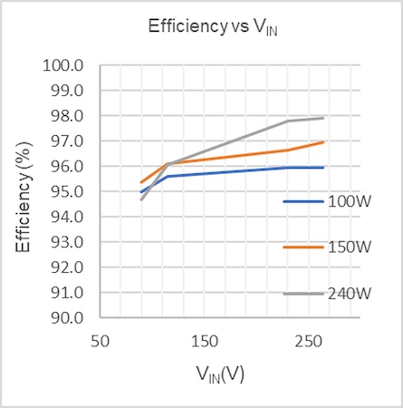
Image used courtesy of ROHM Semiconductor
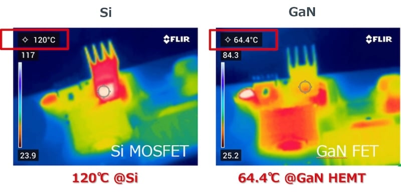
Figure 8. Efficiency plots of the BCM PFC converter utilizing the EcoGaN Power Stage with integrated gate driving IC. Image used courtesy of ROHM Semiconductor
Final Takeaways
The new EcoGaN Power Stage IC directly addresses the massive constraint that comes with the realization of GaN devices: addressing the tight gate drive tolerances. By combining their expertise in GaN development and analog IC design, along with its vertically integrated capabilities, the Power Stage IC offers industry-leading drive voltages.