Facebook
 Google
 GitHub
 Linkedin
Solar Cell Challenges for Indoor IoT Applications
The intensity and spectrum of indoor lighting are vastly different from sunlight. This means indoor photovoltaic (IPV) technology must also be different. This article discusses those challenges and options for IPV cells, test methods, and standards.
The Internet of Things (IoT) market is ever-growing, with many potential applications, from smart home systems to industrial sensors. If this trend continues, billions of low-powered nodes will need to be installed, many inside buildings.
While significant research has focused on minimizing the power consumption of these devices, finding efficient ways to power these billions of units remains a critical challenge. IoT has the potential to save 1.6 Petawatt-hours of energy consumption (through energy management, heating systems, etc). However, IoT devices will introduce energy needs of their own, increasing worldwide energy demand by up to 34 Terawatt hours.
Individual sensors are mostly battery-powered, but relying on disposable batteries poses its own challenges. For example, these batteries may need frequent replacement, which can be wasteful and time-consuming. Often, the ideal use for IoT technology is to monitor and control spaces without human intervention, which is negated if frequent replacement is needed.
Using Indoor PVs for IoT Applications
Indoor photovoltaics (IPV) could be an appealing alternative power source for individual sensors and nodes. As the name suggests, indoor photovoltaics are optimized to absorb indoor light. Some of the benefits of using IPVs over batteries include:
- Longer lifetimes.
- Less human intervention.
- Reduced waste.
- Improved energy-efficiency
- More self-sustaining.
As illustrated in Figure 1, the amount of research devoted to IPV devices has increased yearly as the potential IPV market scales with the IoT market.
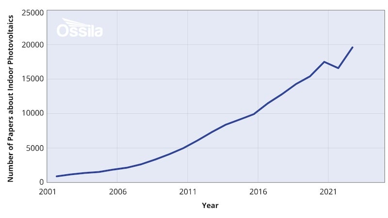
Figure 1. Number of papers published per year linked to the keywords: indoor photovoltaics. Data collected from Google Scholar by Ossila.
The IPV market is expected to exceed 1 billion USD by 2030. This highlights the importance of optimizing and developing efficient IPV technologies to reduce both environmental and financial costs.
Designing Indoor vs. Outdoor PV
Outdoor solar cells are always tested under a standardized solar spectrum, the AM 1.5G spectrum, with an irradiance of 1000W/m2. Testing devices under these conditions will generally provide a good representation of how solar cells will work under sunlight.
However, indoor light is much more variable. There are many different types of indoor light (warm LED, cool LED, fluorescent, etc), but one commonality is that their distribution will mainly be in the visible region, unlike sunlight.
This leads to one fundamental difference when designing solar panels for indoor vs. outdoor use—they have different ideal band gaps.
For solar panels, the ideal band gap is the band gap at which the most electrical energy can be harnessed from the incoming light source. In short:
- The lower the band gap of your material, the more light is absorbed, so the more current is created.
- However, the higher the band gap of your material, the more voltage is generated from this absorbed light.
Achieving maximum power extraction requires balancing these two factors, so your PV material must be as close to its ideal band gap as possible. Outdoor solar panels have an ideal band gap of 1.34 eV, but indoor PV cells have a much higher band gap of 1.8-1.9 eV. You ideally need to choose materials with band gaps near 1.9 eV to make high-efficiency IPV devices.
Additionally, the light intensity of sunlight is much higher than most indoor light sources. Solar irradiation is 1000 W/m2, whereas an indoor LED white light source could have a luminosity of 500 lux, which roughly equates to 1.5W/m2. Therefore, IPVs must perform well in lower light intensities.
C-Si Solar Panels for IPV?
Crystalline-silicon PV is the dominating PV technology used for outdoor solar panels. Silicon has a band gap of 1.1-1.2 eV, so in theory, silicon solar panels can absorb all incoming sunlight below 1100 nm, increasing available current (Figure 2). This is beneficial for outdoor PV as the solar spectrum extends well into the infrared. However, the trade-off is that the voltage generated from c-Si solar panels is limited. For outdoor c-Si solar panels, this voltage loss is offset by the increased current, allowing them to achieve reasonably high efficiencies.
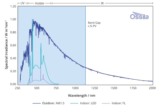
Figure 2. Comparison of the silicon band gap to the spectral distribution of sunlight (AM 1.5), an LED light source, and a fluorescent light source. Image used courtesy of Ossila
However, the spectral distribution of indoor light sources doesn’t extend into the non-visible regions. Why would it? Therefore, if you are using crystalline silicon for IPV, a smaller voltage is generated without the increased absorption or increased current. This leads to lower-efficiency devices. Figure 3 illustrates the ideal band gap for IPV applications.
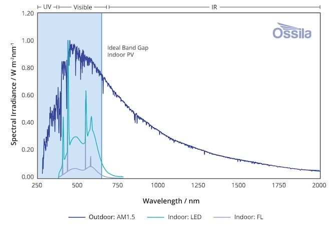
Figure 3. The ideal band gap for indoor photovoltaics, with the spectral distribution of sunlight (AM 1.5G), an LED light source, and a fluorescent light source. Image used courtesy of Ossila
Another problem with c-Si PV is that it performs poorly in lower light intensities. At higher light intensities (such as 1000W/m2 = 1 Sun), any defects that affect device performance (light traps, etc) are masked by the amount of incoming light. In low light intensities, loss mechanisms are more dominant, and device shorting is common. The performance of commercially available c-Si solar panels drops from 15% in high light intensities to 5% in low light intensities (700 lux).
Finally, to be efficient, silicon solar panels must be thick, rigid, and heavy, which limits their use in IoT applications. These limitations suggest that alternatives to silicon solar cells may be better suited for indoor environments.
Other PV Technologies for Indoor PV Applications
Third-generation photovoltaic technologies, such as organic solar cells (OSCs) or perovskite solar cells (PSCs), are promising candidates for IPVs.
Some key advantages include:
- Tuneable band gaps: By varying the composition of perovskite materials or by varying the types of organic material used, the band gap can be adjusted to match indoor light sources, improving efficiency.
- Solution processible: Both OSCs and PSCs are mainly solution-processed. While some air-sensitive components require controlled environments for deposition, such as a glove box, this process is still much less energy and resource-intensive than silicon solar cell production.
- Thin, flexible devices: Easier processing methods and thin active layers mean that you can deposit OPVs and PSCs on a variety of substrates, including polymer substrates for flexible devices, or onto curved surfaces.
- Lower manufacturing costs – solution processing methods could also reduce manufacturing costs which is vital if IoT nodes are to be affordable.
At low light intensities, both PSCs and OSCs perform well. Perovskite materials have low defect tolerances, so they don’t suffer from loss mechanisms as much as c-Si PV. For example, PSCs have achieved a power conversion efficiency of 45% in indoor light conditions using a wide band gap perovskite.
OSC devices also excel under low light intensities due to their high shunt resistance. A PM6:Y6 OPV blend solar cell has achieved a power conversion efficiency of roughly 32% under LED illumination.
Despite their potential, both OSCs and PSCs face challenges related to stability, as they are prone to degradation from environmental factors like heat, moisture, and oxygen. Inert processing and proper encapsulation can mitigate these issues, but further improvements are necessary for large-scale production.
Standardising Indoor Light PV Testing
One of the main challenges in indoor PV development is the lack of standardized testing. This is largely due to the fact that indoor lighting varies so much in both spectral distribution and intensity.
As mentioned earlier, the AM 1.5G spectrum is well-defined and solar simulators are created to closely match this spectrum. In fact, there are many standards written on specifying the exact light sources you should use to test outdoor solar cells (ASTM E927-19, IEC 60904-9:2020, JIS C 8904-9, etc).
In 2023, the IEC introduced Technical Specification 62607-7-2, which outlines methods for testing solar cells under indoor light, but it does not strictly define a spectral distribution.
Testing indoor PVs is further complicated by the fact that indoor light is measured in terms of luminosity, which considers how light is perceived by the human eye, while outdoor testing uses illuminance, which measures the light's power over a given area. This difference makes it difficult to establish a consistent testing protocol.
Introducing some standards is a step in the right direction, but more work is needed to develop precise standards for the testing and performance evaluation of indoor PVs. Establishing such standards will be essential to ensure the consistent, reliable performance of IPV technologies across the industry.
References
Chakraborty, A. et al. (2024) ‘Photovoltaics for indoor energy harvesting,’ Nano Energy, 128, p. 109932.
Mathews, I. et al. (2019) ‘Technology and market perspective for indoor photovoltaic cells’, SSRN Electronic Journal
Michaels, H. et al. (2023) ‘Emerging indoor photovoltaics for self-powered and self-aware IOT towards sustainable energy management,’ Chemical Science, 14(20), pp. 5350–5360.
Steim, R. et al. (2011) ‘Organic photovoltaics for low light applications,’ Solar Energy Materials and Solar Cells, 95(12), pp. 3256–3261.
Featured image background used courtesy of Adobe
Related Content