Facebook
 Google
 GitHub
 Linkedin
A 500 mA Power Op Amp Breakout Board With Precision Current Limiting
Safely drive up to ±500 mA into reactive loads. This compact module employs the LT1970A and offers independent 1% source/sink thresholds and onboard fault diagnostics.
This 500mA Power Op Amp Breakout Board is designed around the Analog Devices LT1970A, a high-current operational amplifier. The board operates on a dual power supply and includes an onboard fault indicator LED for easy diagnostics, with header connectors for power input, signal input, and output that make integration into a larger design simple. Figure 1 shows the assembled board.
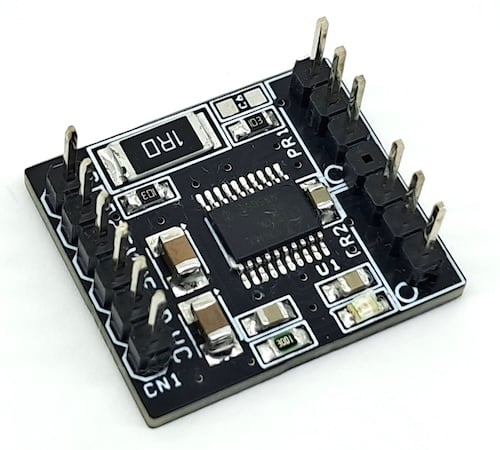
Figure 1. The assembled 500mA Power Op Amp Breakout Board, built around the LT1970A.
The LT1970A is a ±500 mA power op amp with precise, externally controlled current limiting. Separate control voltages program the sourcing and sinking current-limit thresholds to 1% accuracy, and output current can be boosted further by adding external power transistors.
The device operates from single or split supplies from 5 V to 36 V total supply voltage. In normal operation, the input-stage and output-stage supplies are tied together (VCC to V+ and VEE to V−). The output stage can also be powered from independent, lower-voltage rails to reduce power dissipation.
The amplifier is unity-gain stable with a 3.6 MHz gain-bandwidth product, slews at 1.6 V/µs, and can drive capacitive and inductive loads directly.
Specs and Features
- Power supply: ±18 V (dual supply)
- Minimum output current: ±500 mA
- Key IC: LT1970A power operational amplifier
- Independent adjustment of source and sink current limits, 1% accuracy
- Improved stability driving reactive loads
- Operates from single or split supplies
- Shutdown/enable control input
- Open-collector status flags: sink current limit, source current limit, thermal shutdown
- Fail-safe fixed current limit and thermal shutdown
- Slew rate: 1.6 V/µs
- Gain-bandwidth product: 3.6 MHz
- PCB dimensions: 23.18 mm x 20 mm
How It Works
Figure 2 shows the manufacturer's block diagram and test circuit that this board implements. The LT1970A's output stage is protected by two independent current-limit loops. ISNK and ISRC compare the voltage across the current-sense resistor R2 (1 ohm) against the VCSNK and VCSRC control voltages brought in on the PR2 and PR1 headers. This clamps the output drive whenever either threshold is exceeded.
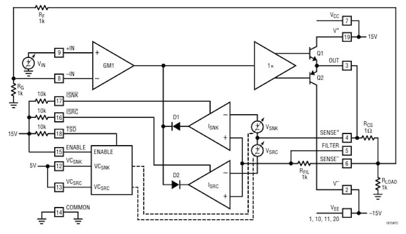
Figure 2. Block diagram and test circuit for the LT1970A, showing the independent source and sink current-limit loops. Image used courtesy of Analog Devices
Because these thresholds are set by external voltages rather than fixed internally, the sourcing and sinking limits can be programmed independently and adjusted in-circuit, with 1% accuracy from the resistor-set thresholds R3 and R4.
Open-collector flags TSD, ISNK, and ISRC report thermal shutdown and current-limit activation back to the host system, while the ENABLE pin puts the amplifier into a low-power, high-impedance output state when pulled low. On this breakout board, D1 (through current-limiting resistor R1) serves as a fault indicator, and C1 through C5 provide local supply bypassing for the ±VCC/VEE rails.
Schematic and Bill of Materials
The full schematic for the 500mA Power Op Amp Breakout Board is shown in Figure 3.
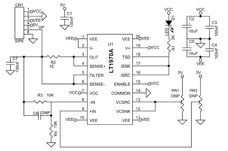
Figure 3. Schematic of the 500mA Power Op Amp Breakout Board.
The bill of materials is shown in Table 1.
Table 1. BOM for the 500mA Power Op Amp Breakout Board.
| REF | DESCRIPTION | QTY | MFG | SUPPLIER | PART NO. |
| CN1 | 6 Pin Male Header, Pitch 2.54 mm | 1 | Wurth | Digikey | 732-5319-ND |
| C1, C3, C4, C7 | 100 nF / 50 V Ceramic, SMD 0805 | 4 | Yageo/Murata | Digikey |
|
| C2, C5 | 47 uF / 25 V Ceramic, SMD 1210 | 2 | Yageo/Murata | Digikey |
|
| PR1, PR2, C6 | DNP | 3 |
|
Digikey |
|
| D1 | LED, Red, SMD 0805 | 1 | Osram | Digikey |
|
| R1 | 3 K, 5%, SMD 0805 | 1 | Yageo/Murata | Digikey |
|
| R2 | 1 Ohm / 1 W, 1%, SMD 2512 | 1 | Yageo/Murata | Digikey | YAG3391CT-ND |
| R3, R4 | 10 K, 1%, SMD 0805 | 2 | Yageo/Murata | Digikey |
|
| U1 | LT1970A | 1 | Analog Devices | Digikey | 505-LT1970AIFE#PBF-ND |
Connections
Figure 4 shows how power, signal, and output connect to the board. Note that PR1 and PR2 are DNP (do not populate) on the stock assembly.
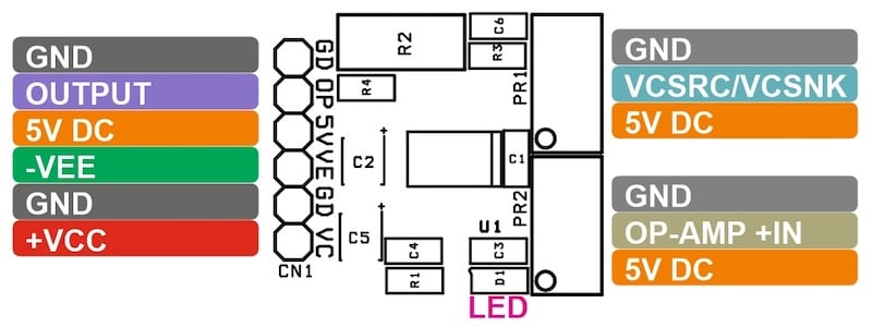
Figure 4. Connection diagram for the 500mA Power Op Amp Breakout Board.
CN1 — Power and Signal (6-pin header, 2.54 mm pitch):
- Pin 1 = +VCC
- Pin 2 = GND
- Pin 3 = −VEE
- Pin 4 = 5 V DC
- Pin 5 = Output
- Pin 6 = GND
PR1 — Sink/Source Current-Limit Set (DNP):
- Pin 1 = 5 V DC
- Pin 2 = VCSRC / VCSNK
- Pin 3 = GND
PR2 — Op-Amp Input Set (DNP):
- Pin 1 = 5 V DC
- Pin 2 = Op-Amp +IN
- Pin 3 = GND
D1 — Fault LED:
- Indicates current-limit or thermal shutdown activation
PCB Files
The PCB measures 23.18 mm x 20 mm. The silk screen, top layer, and bottom layer are shown in Figure 5.
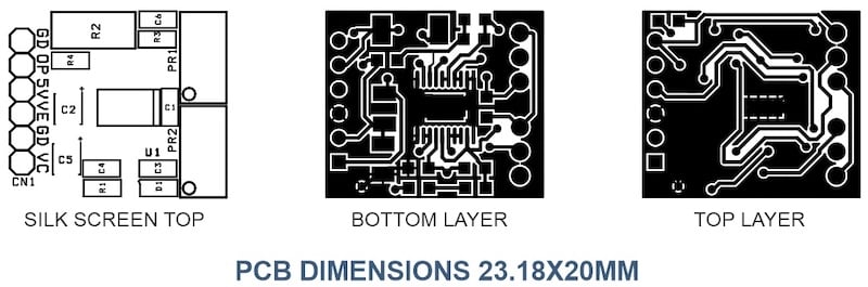
Figure 5. PCB layout for the 500mA Power Op Amp Breakout Board, showing silk screen, top layer, and bottom layer.
You can download the layout files for this project here:
500 mA Power Op Amp Breakout Board Gerber Files
Except where noted, all images used courtesy of Rajkumar Sharma