Facebook
 Google
 GitHub
 Linkedin
The Configurable Matrix Computer: A New Alternative to the von Neumann Architecture
Learn how this new type of AI processor provides a 100x improvement in power and performance over conventional GPUs or MCUs.
Such is the AI world's hunger for compute capacity that the semiconductor industry struggles to keep up with the demand. The problem is not only compute capacity: it is also the huge amount of electricity that AI data centers consume.
These problems for AI hyperscalers are mirrored in miniature for manufacturers of edge products that perform on-device AI, often on battery power. Developers of edge applications want to deploy ever-larger models to benefit from more accurate inference and to inject more intelligence into the system, but are constrained by the slow AI performance and high power consumption of microcontrollers and microprocessors.
The problem is not being solved fast enough by the semiconductor industry's incremental approach to improving AI chips. Most semiconductor companies' approach to AI is to use the conventional architecture of the compute function, then tweak it to make its execution of multiply-accumulate (MAC) operations—the bread and butter of a neural network—slightly faster and more efficient.
But this approach fails to acknowledge that the general-purpose compute architecture used in logic chips for the past several decades is poorly suited to the massively parallel and connected matrix computing operations required by AI systems. The AI industry's hunger for low-power, high-speed matrix computing needs a fundamentally new approach at the silicon level. As we'll see in this article, this is what Ambient Scientific has implemented in its GPX family of AI processors.
Conventional von Neumann Architecture: Inefficient in Neural Networks
The classic von Neumann architecture has been the mainstay of general-purpose computing for decades. This model, which is illustrated in Figure 1, operates by fetching, decoding, and executing instructions sequentially in a cycle that involves a control unit, an arithmetic logic unit (ALU), and memory.
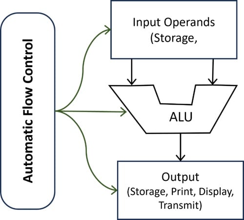
Figure 1. The classic von Neumann architecture handles sequential instructions efficiently.
The von Neumann architecture has dominated because it effectively handles the sequential instructions which underpin conventional software applications. Also, the architecture itself is flexible, simple, and relatively easy to fabricate in silicon. However, the sequential, one-instruction-after-another model of computing which works so well for standard software is a poor fit for AI software. AI models are formed as matrices, not as linear sequences, and call for massively parallel compute operations.
Compiling a neural network's MAC workload to the instruction set architecture (ISA) of a von Neumann-type processor generates huge numbers of operations. For a large language model (LLM) of between 50 billion and 500 billion parameters, a single inference can require from 100 billion to 1,000 billion operations.
And when performing billions of operations, an important determinant of a processor's performance is memory access time, a well understood limitation of the von Neumann architecture. Even after optimizing for performance by tying the fastest SRAM memory to the ALU, inference performance remains disappointing for the largest models, and makes the processor shockingly expensive.
The memory access problem inherent in the fundamental compute block, namely the von Neumann unit, hamstrings parallel computing architectures such as a graphics processing unit (GPU) or neural processing unit (NPU) as much as it does a conventional CPU. Their speed and power consumption still depend on memory access: these digital architectures cannot get enough memory close enough to the ALU. They are limited by the slow speed of DRAM, which cannot be built on the same die as the ALU (a cause of performance/power problems with today's GPUs), or by the limited capacity of fast on-chip SRAM.
Fitting the Compute Architecture to the Compute Task
The problems with implementing neural networking operations on conventional compute architectures have led computer scientists to explore a different approach: the systolic array, which is shown in Figure 2.
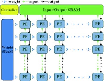
Figure 2. A typical implementation of a systolic array will run into the same problems as the von Neumann architecture.
This is a much better match for the interconnected, multi-layered structure of a neural network. However, previous attempts to implement a systolic array in silicon have struggled with the practical implementation of such a densely interconnected fabric. In addition, the physical separation of memory from compute blocks causes the same problem of memory access—reducing throughput and increasing power consumption—as is found in the von Neumann architecture.
The systolic array is an effective solution to the problem of mapping the compute architecture to a neural network's topology, but what is required to implement it is innovation at the silicon level. This is what Ambient Scientific has achieved with its DigAn technology.
A New Kind of AI Processor: The Configurable Matrix Computer
The DigAn technology has enabled Ambient Scientific to create a configurable matrix computer at chip level. This fundamentally new approach includes a new type of compute unit, the analog MAC. This block does the work of the von Neumann architecture's ALU and memory units (see Figure 3).
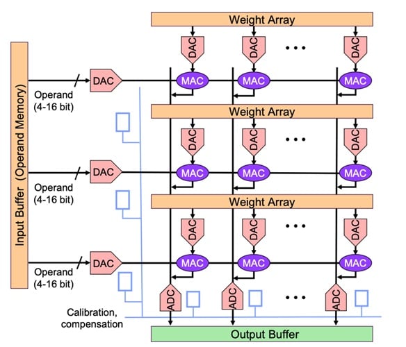
Figure 3. The analog MAC enables in-memory computing.
The analog MAC is optimized for AI systems, in which MAC operations represent 95% of the compute workload. It enables in-memory computing, thus solving the von Neumann architecture's problem of physical separation between the memory and compute blocks. This is thanks to another Ambient Scientific innovation, the HyperPort 3D memory architecture, which enables vertical stacking of memory elements at each MAC unit.
The second weakness of the von Neumann architecture in neural network operations is the vastly inefficient way in which it compiles a neural networking model into instructions. We solve this by creating a matrix computer. It arranges analog MAC blocks to mirror the topology of a neural network.
Each DigAn unit is a single monolithic circuit that computes an entire layer of neurons in a single cycle. As shown in Figure 4, multiple layers of DigAn circuits can be scaled up into a matrix computer that mirrors the structure of a neural network.
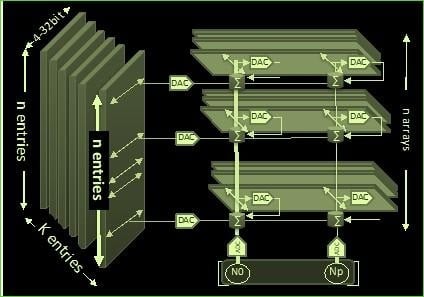
Figure 4. The Ambient Scientific matrix computer, built from multiple layers of DigAn circuits.
The practical result of this is an astonishing improvement in instruction cycle efficiency: just a single DigAn compute block can compute a 1 × 32 × 8 matrix in one cycle, compared to 38,600 cycles for an AI processor based on a conventional silicon architecture.
Multiple layers of these DigAn blocks form a matrix computer: 32 layers of a typical 1 × 32 × 8 neural network matrix would require 1,235,200 cycles for a conventional compute architecture to perform. In a DigAn matrix computer, this requires just 32 cycles.
When reducing neural networking operations from 1,235,200 cycles to 32 cycles, the application benefits from remarkable improvements in performance and power: more than 100 times better performance than a typical MCU with the same power consumption, or the same performance as a typical GPU but using less than 1% of the energy.
New Silicon Technology Realized in GPX Family Chips
The power and performance breakthrough described above stems from Ambient Scientific's commitment to adopting a novel processing architecture and developing entirely new silicon technology for its implementation. To enable high-speed, low-power AI, this core technology must be readily accessible to embedded systems engineers. Furthermore, the chips must be accompanied by development environments for compiling trained AI models to devices.
The GPX chip family provides this DigAn implementation. Within GPX products, DigAn blocks are combined into AI processor cores (see Figure 5) that scale to accommodate varying application requirements. These are known as MX8 cores.
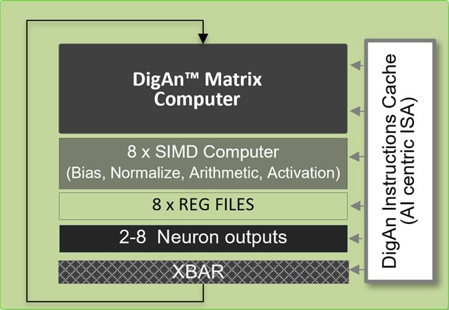
Figure 5. Each MX8 core is a self-contained neural network processing unit.
As of the end of 2025, the GPX family consists of the GPX10 and GPX10 Pro. The GPX10 Pro which is the newer of the two, employs two clusters of five MX8 cores to deliver high inference performance at minimal power. As shown in Figure 6, it is a complete system-on-chip (SoC), managing control and sensor interface operations via its Arm Cortex-M4F controller core.
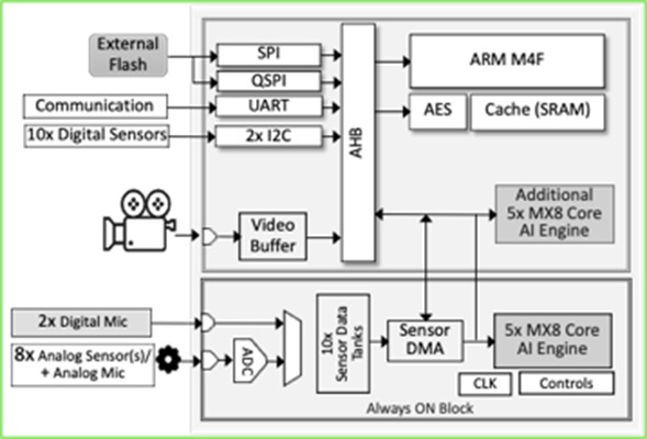
Figure 6. The GPX10 Pro is a complete SoC, not just an AI processor.
Despite the GPX device family's entirely novel underlying technology, engineers can continue to use tried and trusted frameworks and tools for model training and development. GPX processors support major machine learning frameworks such as TensorFlow, PyTorch, Keras, and ONNX.
Ambient Scientific's Nebula software development kit for GPX devices also provides complete model training toolchains. It includes tools for translating AI models to MX8 cores, as well as configuration tools for middleware—device drivers and real-time operating systems, for example—running on the device's Cortex-M4F core.
Engineers basing edge AI designs on the GPX10 or GPX10 Pro can therefore utilize familiar platform software for model development and maintain the design productivity they expect from conventional MCUs when using the Ambient Scientific IDE.
Wrapping Up
Rather than adapting a general-purpose computing architecture that is fundamentally unsuitable for AI functions, the new GPX chip family employs silicon architecture inherently designed for neural networking. Because MX8 AI cores scale readily, the product roadmap envisions future GPX devices expanding to 8,000 cores for data center servers and supercomputers.
For AI system developers who prioritize performance and power consumption, these new chips and the DigAn architecture herald a transformative era for AI processing and neural network operations.
All images used courtesy of Ambient Scientific
Related Content