Facebook
 Google
 GitHub
 Linkedin
The New Moore’s Law: Why Optical Computing Could Redefine Scaling for AI
Optical computing is the "New Moore's Law" for AI. It solves electronic scaling limits, offering higher speed, lower power, and efficiency gains proportional to problem size for matrix operations.
For more than half a century, Moore’s Law has guided the semiconductor industry, setting the pace for how fast, efficient, and affordable computing could become. By doubling transistor density roughly every two years, engineers exponentially increased processing performance while reducing costs, fuelling everything from mobile devices to the rise of the Internet.
But AI has broken the curve.
The End of Scaling as We Know It
Training and deploying large neural networks requires compute resources that grow faster than transistor improvements can sustain. State-of-the-art models are measured in hundreds of billions of parameters, demanding thousands of GPUs and megawatts, if not gigawatts of power. Even with semiconductor process shrinks and specialized accelerators, the real performance gains have plateaued while power consumption continues to climb.
This creates a paradox: we have more data, better algorithms, and greater demand than ever, yet we are running out of room to scale using electrons alone. Data centers already consume approximately 1-2% of global electricity, with AI workloads driving exceptional growth. By 2028, U.S. data centers alone could consume 12% of the nation's power supply, triple current usage.
This is precisely the moment when optical computing becomes essential.
A Different Physics of Computation
Optical computing replaces electrons with photons for certain computational tasks, most notably the matrix multiplications that are at the heart of (and dominate) AI workloads. Rather than moving charge through transistors and on-chip resistive connections, optical systems encode data in beams of light beams to perform the same mathematical operations using the physical properties of light itself.
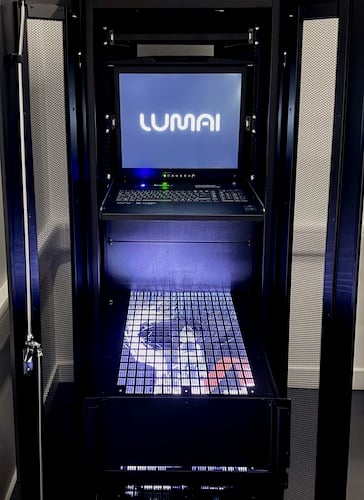
Optical compute performs AI acceleration much faster than using electronic systems alone.
Photons offer fundamental advantages over electrons. Because they do not interact the way electrons do, they propagate without generating heat through resistance, enabling ultra-low energy and high-bandwidth computation. Moreover, light can easily support parallelism where multiple beams of light can be used to process information simultaneously.
This is not a new idea, optical computing research stretches back decades, but only recently have we reached the technological maturity, and application demands to make it practical. Optics is now truly embedded within data centres, initially for longer distance connectivity across racks but now also for short-distance connections within a rack.
With optical interconnect in place comes optical switching—which has (for example) been deployed by Google for close to ten years. Advances in silicon photonics, integrated optoelectronics, and the convergence of analog computation with AI’s probabilistic algorithms have made this a defining moment for the field of optical computing.
Two Paradigms: Integrated Photonics vs. 3D Optics
Not all optical computing approaches are the same. The field has evolved along two distinct architectural paths, each with unique advantages and trade-offs.
Integrated photonics confines light within waveguides (narrow channels etched into silicon or other materials) enabling compact, chip-scale designs similar to traditional integrated circuits. This approach offers good integration with existing semiconductor manufacturing. However, integrated photonics faces inherent constraints when it comes to compute: optical losses accumulate as light travels through waveguides, thermal crosstalk between densely packed components degrades performance, and the two-dimensional nature of chip layouts limits the degree of parallelism achievable.
3D (free-space) optics takes a fundamentally different approach by allowing light to propagate through three-dimensional space rather than being confined to waveguides. This eliminates the loss and crosstalk issues of integrated photonics while unlocking true parallelism. In a free-space optical system, light beams can be split, modulated, and recombined across all three spatial dimensions simultaneously, enabling matrix operations that would require thousands of sequential steps in electronic or integrated photonic systems to be performed in a single pass.
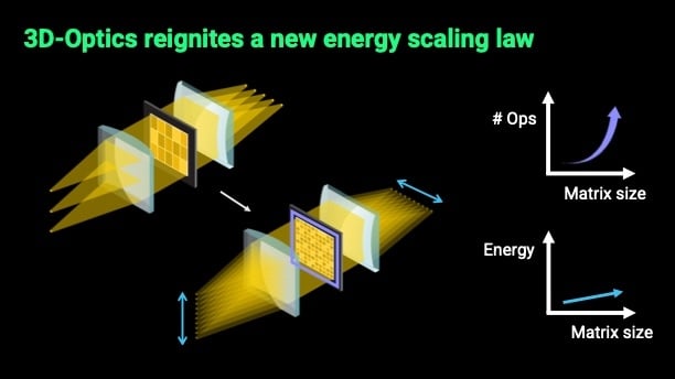
By utilizing 3D dimensions, optical compute offers a new scaling law – where efficiency increases as performance increases.
Lumai, an Oxford, UK–based company, is developing an AI accelerator that applies this 3D optical approach. In its architecture, input vectors are encoded by arrays of light sources and expanded through 3D space using lenses to span the full width of the matrix. The matrix weights are implemented on spatial light modulators—such as electronic display panels—where each pixel’s intensity modulates the light passing through it, effectively performing multiplication.
Final lenses then combine the modulated light to form the output vectors. In this scheme, the multiply–accumulate operations—the primary computational bottleneck in AI inference— use virtually no energy; power consumption is largely limited to the light sources and conversion, matrix updates, and the digital control electronics.
This 3D optical approach can be implemented using commercially available technology: lasers, lenses, etc which can be optimised for optical compute, making it cost-effective to manufacture at scale. More importantly, it offers a clear scaling path: as components become denser and more precise, the number of parallel operations grows quadratically, rather than linearly, providing headroom for continued performance improvements.
The Architecture of Optical AI Accelerators
Optical computing systems do not replace general-purpose processors, they augment them. The key insight is that AI inference workloads are dominated by matrix-vector multiplications, which can account for 80-90% of compute cycles - operations that optical systems can perform with exceptional efficiency.
A hybrid architecture combines optical cores for matrix operations with digital electronics for everything else.
Optical Core: Matrix-vector multiplication using light.
Digital Control: ASIC or FPGA-based controllers handle non-linear activations, normalization, data formatting, and system orchestration.
The result is a co-processor that slots into standard data center infrastructure via PCIe slots, providing seamless integration with existing software stacks while delivering order-of-magnitude improvements in speed and energy efficiency for inference workloads.
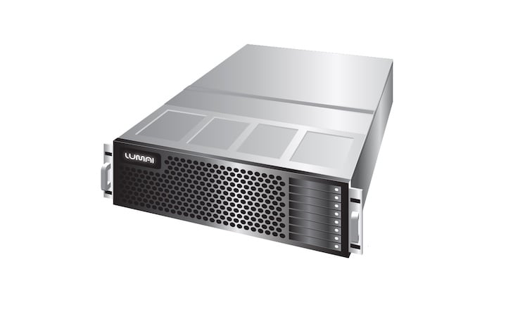
Optical compute-based AI accelerator uses standard data center form factors.
Recent demonstrations have validated this approach. Microsoft Research's analog optical computer (AOC) achieved 100-fold improvements in energy efficiency for optimization problems and AI inference tasks, solving complex banking transactions and MRI reconstruction problems that would be impractical with conventional computing.
Lumai's architecture extends these concepts significantly. The company’s roadmap aims for up to 50× performance improvements over silicon-only systems while operating at roughly 10% of the power consumption – levels of AI Tokens-per-Watt efficiency that are difficult to achieve with silicon alone.
Trading Precision for Power
Because optical systems operate in the analog domain, signal levels can be adjusted allowing system designers to tune energy consumption directly: by lowering signal amplitude, overall compute energy can be reduced. When combined with optimized quantisation algorithms that adapt model precision to analog signals, it becomes possible to cut power dramatically while maintaining model accuracy. In this way, the analog nature of optical computing provides additional degrees of design freedom.
Memory vs Compute Bottlenecks in AI
The relationship between memory bandwidth and compute capacity in AI workloads is more nuanced than often portrayed. While it is commonly said that AI workloads are memory bound, this varies significantly depending on the specific operations, model architecture, and deployment scenario.
Dense matrix multiplications in attention layers and fully connected networks are compute-intensive and this is where optical computing can shine. An entire matrix-vector operation can occur in one cycle in light, dramatically reducing both latency and energy consumption compared to digital systolic arrays that require hundreds of cycles and extensive data movement.
The optimal system-wide solution combines technologies matched to each operation type. Optical accelerators tuned to compute applications can handle the heavy matrix multiplications that dominate modern transformers, for example at the pre-fill stage, while versions with additional memory could be deployed for memory-bound operations. This hybrid approach targets bottlenecks where they actually exist, rather than applying one solution universally.
The Physics of Optical Scaling
The most striking property of optical computing, especially when implemented in 3D, is that its efficiency improves as the problem size grows. This contrasts sharply with traditional electronics, where larger or faster chips consume disproportionately more power and deliver diminishing efficiency returns.
Consider an optical matrix–vector multiplication, the core operation in many AI models. The optical energy required scales linearly with the vector width N, but the computational throughput scales as N2 because each of the N outputs depends on all N inputs.
The result is a remarkable scaling law:
Energy $$ \propto $$ N, Performance $$ \propto $$ N² → Efficiency $$ \propto $$ N
In other words, the larger the optical computation, the more efficient it becomes.
Unlike in conventional silicon chips, scaling in optics does not depend on transistor miniaturization, it depends on increasing optical vector width, improving optoelectronic conversion efficiency, and optical clock rates. The difference is that there is much more room to grow, unlike in traditional electronic-based solutions where the answer is to add more transistors, much more complexity, power and heat.
Continuing the Scaling Journey
Optical computing opens multiple axes of scalability beyond what electronics can offer:
- Vector Width Scaling – As explained, efficiency improves with matrix size. Larger optical systems achieve better performance-per-joule, making them ideal for data center and large-model inference applications.
- Component Efficiency – Each generation of modulators, detectors, and light sources improves the electro-optic conversion efficiency. These gains directly translate into system-level energy savings.
- Higher Optical Clock Rates – Optical signals can be modulated and detected at tens or hundreds of gigahertz. As optoelectronic interfaces advance, clock frequencies will continue to rise without the thermal penalties of electronic switching.
Together, these trends suggest that optical computing won’t just catch up to silicon, it will keep scaling long after transistor improvements plateau.
A New Law for a New Era
If Moore’s Law defined an era of electronic miniaturization and densification, the next era may be defined by computational diversity, using the best physical medium for each task. Photons don’t replace electrons; they complement them - using light for key AI workloads and unlocking performance scaling that better matches the trajectory of AI.
In this emerging paradigm, progress is measured not by transistor counts but by what is achieved through harnessing the properties of optical speed and parallelism for AI computation. As these grow, so too does the potential to perform more work per joule.
The result is a computing landscape where scaling continues, not through smaller transistors, but through smarter physics.
All images used courtesy of Lumai
Related Content