Facebook
 Google
 GitHub
 Linkedin
Three Research Teams Take Different Routes to Control Light
Papers from École Polytechnique, Seoul National University, and Harvard tackle optical gain, on-chip buffering, and component footprint.
An international team led by École Polytechnique reported the first all-optical photonic time crystal in Nature on July 29, cutting plasmonic losses by more than 50% in a terahertz metamaterial driven at picosecond timescales.
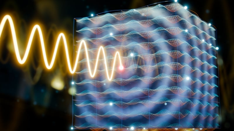
École Polytechnique and its partners claim they are the first to realize an all-optical photonic time crystal. Image used courtesy of École Polytechnique
Two weeks earlier, Seoul National University and the University of Seoul published a design for a photonic integrated circuit that slows and delays light on command, addressing the absence of a workable optical buffer. And Harvard SEAS and the Max Planck Institute for the Science of Light handed component design to an optimizer, producing silicon nitride multiplexers up to 500 times smaller than conventional layouts.
All three attack the same underlying problem from different angles: light is hard to hold still, hard to amplify on a chip, and expensive in area.
École Polytechnique Modulates a Material Faster than Light Oscillates
Photonic crystals control photons through a periodic spatial pattern. The École Polytechnique work, in collaboration with Collège de France, CNRS, and Helmholtz-Zentrum Dresden-Rossendorf, translates that periodicity into time.
The device is a plasmonic metamaterial: micrometer-scale gold crenellations over an insulating layer over indium antimonide, forming cavities that trap terahertz photons against surface plasmons in the semiconductor. Driving it with high-field, phase-stable pulses from HZDR's TELBE source modulated the carriers' effective mass to up to 80% of their rest mass, achieving a near-unity modulation depth within a single optical cycle.
Spectroscopy revealed that the system crossed into the photonic time-crystal regime through an exceptional point, where two Floquet-driven optical eigenmodes coalesce. The emergent gain in that regime halved the metamaterial's plasmonic losses, and the authors predict that plasmonic lasing is within experimental reach. Notably, the demonstration required a superconducting linear accelerator to produce the drive pulses.
SNU Develops Programmable Buffer for Light
Optical routing has no equivalent of a RAM buffer, because photons travel at a fixed speed and can't be parked. Coupled-resonator-induced transparency is one workaround: interference among linked resonators transmits light in a narrow band while slowing its group velocity. A CRIT structure's behavior is fixed at fabrication, though, so a longer delay or a different operating band means designing a new device.
The SNU team treats CRIT's bright and dark modes as a single degree of freedom and adds two controllable loop couplers. That creates control over passband bandwidth and shape, delay, and transmission across a multi-resonator system rather than within a single ring. Pulse propagation speed can be adjusted while the circuit is running. Frequency conversion falls out of the same mechanism without additional components.
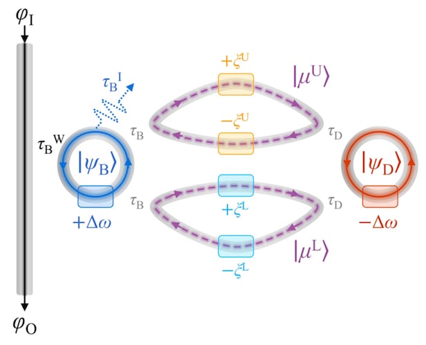
The structure of the programmable CRIT photonic integrated circuit. Image used courtesy of SNU
Ultimately, this is a design principle validated through three-dimensional electromagnetic simulation on a silicon nitride platform, alongside a robustness analysis that covers material loss, resonator quality variation, backscattering, coupling fluctuations, loop coupler phase error, and thermal crosstalk. No device has been manufactured yet, but the researchers say practical implementation and experimental validation will come next.
Harvard Turns to Algorithmic Light Control
Harvard SEAS and the Max Planck Institute for the Science of Light designed, fabricated, and tested three classes of silicon nitride components for their Nature Communications paper. The smallest of them, a three-port, wavelength-division multiplexer, occupies 5 µm x 5 µm.
A directional-coupler version of the same function needs hundreds of micrometers of coupling length before anything else is counted. Here, the team specified what the light should do and handed the search to a gradient-based optimizer.
Everything sits on thick silicon nitride, 400 nm to 800 nm, a platform with low loss and useful nonlinearity that, until now, has carried no component library beyond hand-engineered designs. Mode-division multiplexers ranged from 8 µm x 8 µm to 15 µm x 10 µm, with an insertion loss of approximately 1.5–2 dB for both types. Reflectors occupying 11 µm x 2.8 µm achieved 98.5% peak reflectivity and, when paired into Fabry-Perot cavities, reached a loaded finesse of 162 and a Q near 210,000. Ring resonators on the same chip measured intrinsic Q above 20 million at 8 dB/m propagation loss.

The researchers' photonic microchip prototype beside a 10-euro-cent coin for scale. Image used courtesy of Tony Bi/MPL via Harvard
Harvard's release puts the size reduction at about 500-fold. The paper splits that number: it belongs to the mode-division multiplexers, while the wavelength multiplexers range from roughly 50 to 300 times. Fabrication costs the devices' measurable performance too, with O-band crosstalk coming in at 3 dB against 8 dB in simulation, which the researchers attribute to imperfect sidewall angles and incomplete gap filling. The optimizer was held to 80 nm to 100 nm minimum feature sizes so the designs would survive a foundry process, though these particular chips were written by e-beam lithography at Harvard's Center for Nanoscale Systems.
Related Content