Facebook
 Google
 GitHub
 Linkedin
Using a Silego GreenPAK to Build a Temperature Sensing System
In this project, we'll test how the Silego GreenPAK can be used to build a temperature-sensing system.
In this project, we'll test how the Silego GreenPAK can be used to build a temperature-sensing system.
The purpose of this experiment is to test the usability of a GreenPAK device in a temperature-sensing application, specifically for CPU processors where the temperature domain is 25°C to 100°C. The temperature-sensing system uses a remote temperature sensor 2N3904 (diode-connected) and control logic that is implemented in the GreenPAK device. The goal is to achieve a +/- 1°C internal temperature accuracy using an SLG46537 chip.
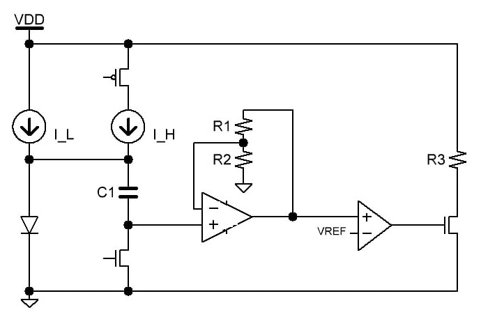
Figure 1. Application circuit for the temperature sensor that implements two-current method
Theory
The Two-Current Method
The two-current method is a voltage subtraction method using two current sources, a diode, capacitor, and FET switches (see Figure 1). It is designed to amplify the voltage difference on the diode induced by two different currents I_L and I_H.
The forward voltage of the diode varies based on the current-induced e-field across the diode. By subtracting the forward voltage at two known currents, we can eliminate common variables such as offset and saturation current. The forward bias current, ID, of a diode is related to the saturation current Is and forward voltage VD by the equation:
Where η is the ideality factor of the diode and VT = kT/q. k is the Boltzmann constant and q is the electron charge constant. For this example, I_H will be bias current I1 and I_L will be bias current I2. Their forward bias current equations are thus respectively:
By dividing the two-forward bias current equations, we eliminate saturation current and reduce the input current variables to a scalar factor N.
I1⁄I2 = N = e(V1-V2)/ηVT
If N is known, then by measuring the difference between V1 and V2, we can calculate temperature T.
ln(N) = (V1-V2)q/(ηkT)
T = (V1-V2)q/(ηkln(N))
Ideality Factor η
While k and q are constants and do not vary from part to part, the ideality factor η does vary between the values 1 and 2. The closer this value is to 1, the more that carrier diffusion dominates. The closer this value is to 2, the more recombination dominates. The higher this value, the more erroneous the temperature measurements because temperature would highly affect recombination but not diffusion. [1]
When picking a remote temp diode, remote diode-connected transistors—BJTs where the base-collector junction is shorted—are better than rectifier diodes because their ideality values are specced. Almost all BJT transistors have an ideality factor close to 1.
Other important parameters include the forward current gain β and series resistance Rs. The forward current gain varies with temperature and collector current and the series resistance presents a constant offset at all temperatures. It is recommended to choose a device whose β doesn’t vary between the two currents I_H and I_L.
Experiment Circuit
The purpose of the experiment is to measure the deviation in temperature in general by testing a few points: 40°C, 60°C and 80°C.
Figure 2 shows a block diagram of the application circuit used in the experiment.
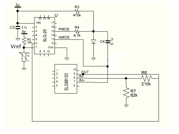
Figure 2. GPAK block diagram for the temperature sensing application circuit
Resistors R3 and R4 provide currents I_H and I_L from Figure 1. The switches NMOS and PMOS are internal to the GreenPAK (PIN 13 and PIN 15). The internal GreenPAK design is shown in Figure 3 and gives 10ms Update Time for this sensor.
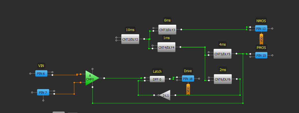
Figure 3. Internal GPAK Design
The capacitor C4 is charged with I_L when the NMOS is pulled low and the PMOS is floating. C4 is charged with I_H when the PMOS is pulled high and the NMOS is floating. The control logic of the system is programmed to provide a dead band time—between the NMOS and PMOS turn-on time—to get the voltage difference on C4.
This difference enters IN+ input of the op-amp (Silego’s SLG88103). A waveform of voltage across C4 is shown in Figure 4.
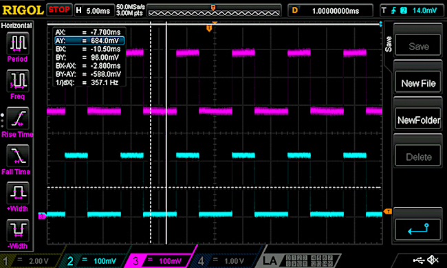
Figure 4. Waveform of voltage across C4
PIN 7 of the GPAK device is connected to a voltage divider with a variable resistance (a trimpot potentiometer) which is used for adjusting the switching voltage of the analog comparator ACMP0 in the internal GPAK design. The switching voltage is the moment when the voltage on PIN 7 reaches the voltage on PIN 6 (the op-amp output voltage). The output voltage of the op-amp (and, consequently, the switching voltage of ACMP0) is different for different temperatures.
Therefore, in the experiment, the resistance of P1 is tuned until the switching moment occurs. Based on the measured resistance of the potentiometer P1, the ACMP0 switching voltage (Vref) can be calculated.
Results
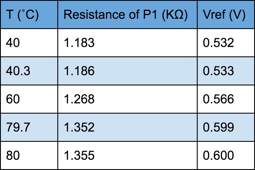
The error induced by GPAK (the temperature measurement accuracy) is measured by testing the output across multiple devices (three GPAK devices). The test results for three sensor circuits with only one different component (GPAK5 device) are recorded in Tables 1, 2, and 3, where:
- The temperature in the oven is measured with a thermocouple.
- The resistance of P1 is measured with a fluke multimeter.
- Vref values are calculated based on the resistance value of P1.
Table 1. GPAK5_1
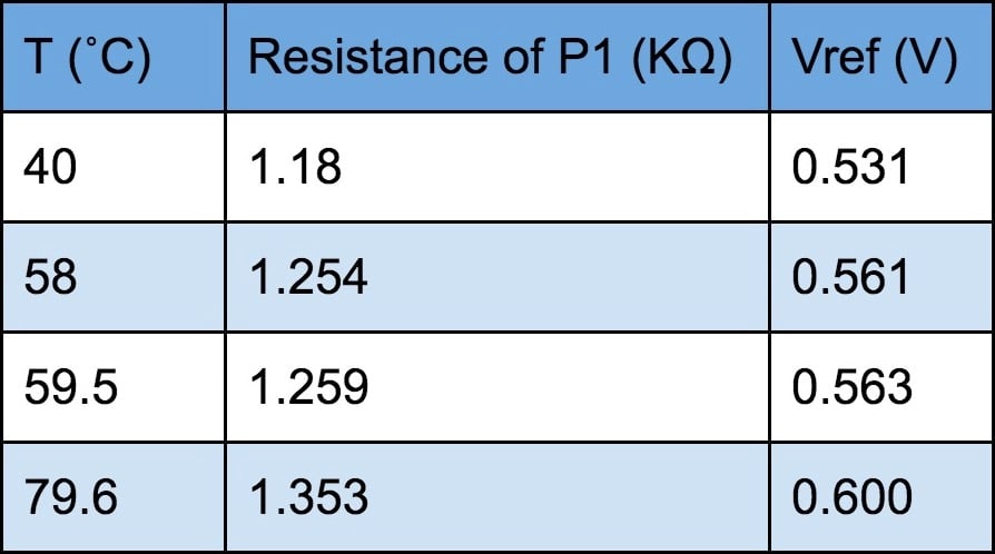
Table 2. GPAK5_2
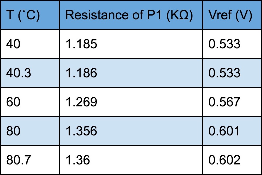
Table 3. GPAK5_3
The results are further summarized with graphs in Figure 2.

Figure 2. Graphs based on the measurements of three sensors with different GPAK device
Figure 2 shows that the sensors 2 and 3 give linear graphs that overlap while the sensor 1 gives the line that is very close to the presented linear trendline for sensor 1.
The slope of the graphs for sensor 2 and 3, as well as the trendline for sensor 1, is 1.7mV per 1°C (between T=40°C and T=80 °C). The maximum difference among the measurements of the three GPAK devices is 2mV. This means GPAK introduces a part-to-part error around 1°C.
Error Sources
Analog Comparator
The GreenPAK design suggests that the part-to-part variation would most likely occur from the analog comparator component (ACMP0). The ACMP0 settings in the design for this application are as follows:
- IN+ source: pin6
- IN- : Ext. Vref (pin7)
- IN+ gain=1
- Hysteresis: disable.
The offset voltage of ACMP (and, consequently, the switching voltage) changes with temperature and supply voltage. The conclusion of the experiment is based upon the measurements of a GPAK sample of three—too few for statistical analysis.
As a typical representation, we can use Silego’s ACMP Offset Voltage char data, which is based on a set of 35 components tested over temperature and voltage. The component ACMP offset results for Ext.Vref=600mV and 5V supply voltage, measured at room temperature are shown in Table 4.
Table 4
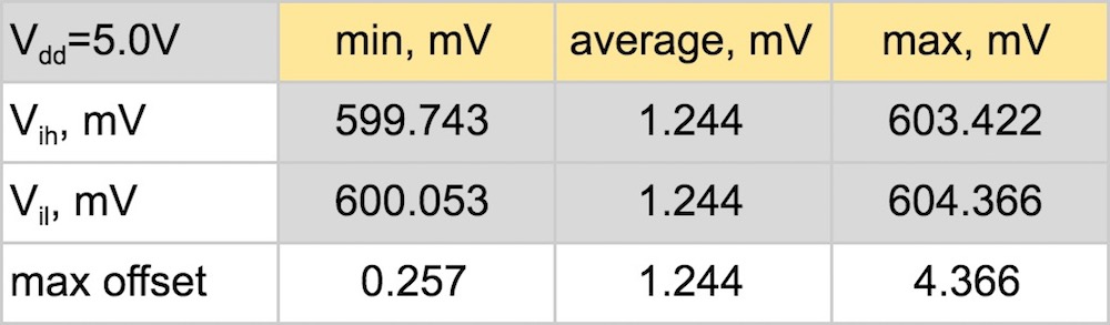
Table 4. ACMP offset testing for Ext.Vref=600mV_AutoPWR, 35 components, Room Temperature
Silego’ s Voffset calculations are based on the equation below:
The test results based on 35 components suggests that the ACMP offset can be up to 4.366 mV which can introduce the error up to 2.5°C.
The 2N3904 Component
Transistor parameters that affect temperature measurements accuracy (remote accuracy) are the forward current gain β (I) and series resistance Rs. Based on the Microchip lab data for 2N3904, those parameters have a small effect on temperature measurement accuracy over the entire sensor’s sourced current range (4.5-920uA). [1]
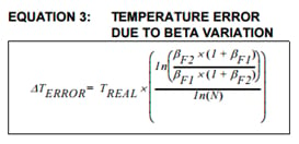
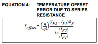
Figure 3 shows the typical beta values of transistors tested by Microchip and can be used as a typical representation for the limited quantity of 2N3904 transistors. [1] Equation 3 gives the temperature error due to illustrated beta variation around 0.02°C at 80 °C. Similarly, using Microchip’s data for Rs of the set of 2N3904 (around 0.7 Ohm) with Equation 4 gives a temperature error due to Rs of around 0.8°C. [1]

Figure 3. Typical beta values for 2N3904 transistors at 23°C (the Microchip lab data)
Op-Amp Consideration
SLG88103 voltage offset is typically 0.35mV (up to 2.4mV for VCM close to VSS (ground)), plus typically 0.16mV (T=80°C) for adding offset drift with temperature. Typical values introduce a small error coming from the op-amp for this application. However, having in mind the maximum offset value the SLG88103 op-amp can introduce more than 1 °C error.
Conclusion
The temperature sensing system that is used in the experiment gives the output gain of 1.7 (mV/°C).
The test results based on a sample of three GreenPAK devices suggest that the implementation of GreenPAK in a temperature sensing system alone introduces an error around 1°C.
Key features of the sensor are based on the experiment’s results where the temperature domain is for the remote sensor while the internal temperature system with GreenPAK was kept at room temperatures during the experiment. To view the app note and design file for this project, click here.
GreenPAK Key Features
- Temperature domain (25°C - 100°C)
- Accuracy
- ±1°C Remote Temperature Accuracy (accuracy of 2N3904 sensor)
- ±1.5°C Internal Temperature Accuracy
- 1.7V-5.5V Supply Voltage
- 10ms Update Time
- 1.7 (mV/°C) Output Gain
- 29μA Quiescent Current
Sources
[1] Remote Thermal Sensing Diode Selection Guide, SMSC AN12.14
Related Content