Facebook
 Google
 GitHub
 Linkedin
What Does the Future Hold for SiC Semiconductors?
This article looks ahead to what needs to be next for SiC, where it might be applied, and how it could become the dominant force in power.
Over the past three years alone, as a semiconductor technology, SiC has grown to the level that it can compete with silicon. Now in its 3rd generation, SiC delivers performance with a growing number of applications.
With the pace of innovation in sectors like EV, renewable energy and 5G increasing at a rapid rate, to meet consumer and industry demand, power engineers are increasingly looking for new solutions to give an edge in efficiency and cost savings as well as functionality.
Crystals of silicon carbide can be things of beauty as ‘Moissanite,’ after Dr. Ferdinand Henri Moissan, who found the material in the remnants of a meteorite in Arizona in 1893. Today, gems can be formed from silicon carbide which is difficult to distinguish from diamond and even more resistant to heat. Crystals are also now grown industrially as the basis for silicon carbide (SiC) wafers for a hugely successful new class of semiconductors — perhaps fab technicians peer into SiC ‘crystal boules’ and wonder what is next for devices using the material?
The 3rd Generation of SiC Technology
Let's recap where SiC technology is today and how well it competes with traditional silicon solutions. The basic material characteristics compared with silicon are shown in Figure 1 – values closer to the edge are better.

Figure 1. A comparison of Si and SiC material characteristics.
This summarizes the advantages that SiC gives: wider bandgap which leads to much higher critical breakdown voltage with higher electron velocity allowing faster switching. Die size for a given voltage rating can be much smaller giving low on-resistance which, coupled with the dramatically better thermal conductivity, gives low losses and cooler operation. The small die size also reduces device capacitances, in turn lowering switching losses, with thermal stress anyway reduced by the inherent high-temperature capability of SiC.
When implemented as a SiC FET, a cascode arrangement using UnitedSiC’s approach of co-packaging a SiC JFET with an Si-MOSFET, a normally-off device results with a fast, low-loss body diode, high avalanche energy rating and self-limiting current under short circuit conditions. The SiC FET has an easy gate drive, compatible with older Si-MOSFETs and even IGBTs so, with compatible packaging available, there is an easy upgrade path from the older device types.
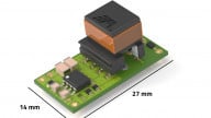
For high switching frequency applications, the low-profile DFN8x8 packages are also now available which minimizes lead inductance and is therefore ideal for hard and soft switching applications such as LLC and phase-shift full-bridge converters.
Using the technology, a barrier has recently been broken by devices in UnitedSiC’s UF3C range which are the first SiC FETs to achieve less than 10 milliohms RDS(ON) in the 1200V class of devices, in a 4-lead TO-247 package with Kelvin gate connection.
SiC wafers used in UnitedSiC have advanced to the six-inch size, with the economy of scale allowing parity with silicon pricing levels and use in mass-market applications, as well as in cutting edge innovative products.
Drivers for Further SiC FET Improvement
SiC FETs are approaching the ideal switch but the market still asks for more; EV inverters require best possible efficiency for increased driving range; high power DC-DC, as well as AC-DC converters in data center/5G applications must dissipate as little power as possible to minimize energy loss, footprint and costs; industry wants smaller and more efficient motor drives for better factory space utilization. The list goes on, with the headline requirement – better efficiency. Other new applications for SiC have also opened up that leverage some of the SiC benefits – solid-state circuit breakers, for example, can now be very low loss at high current levels and even linear power circuits such as in electronic loads are better with SiC devices with their extended safe operating area (SOA).
As system engineers appreciate the opportunities to reduce size and cooling requirements while saving energy and hardware costs, they want more of the same, along with devices with wider application such as higher voltage and current ratings and more package options.
Comparing Current and Possible Future Devices
When comparing current devices and what they might evolve to, individual parameters are not necessarily enlightening – a sub-ten milliohm device is not so impressive rated at 100V but would be state of the art at 1200V; equally, low RDS(ON) at 1200V is not so useful if the die area is large, leading to high capacitances and consequent switching losses. So it is useful to use agreed ‘Figures of Merit’ (FOMs) such as RDS(ON).A, the product of on-resistance and die area; a low value combines measures of low resistive and switching losses, and number of die per wafer, which reduces cost.
EOSS, the energy required to charge the device output capacitance is important for low switching loss and again a useful direct FOM for overall losses is RDS(ON).EOSS,
Parameters for SiC Improvement
Clearly SiC is a huge improvement over other switch types for critical FOMs but what is the scope for even better performance? Other parameters also need to be considered that might trade-off against FOM improvements. Figure 2 shows some, and the arrows indicate the direction of movement for better performance. BV is critical breakdown voltage, COSS is output capacitance, Qrr is reverse recovery charge, ESW is energy loss in switching, Diode Surge is the body diode effect peak current rating, SCWT is short circuit withstand rating, UIS is unclamped inductive switching rating and RthJ-C is the junction to case thermal resistance.

Figure 2. SiC FET characteristics and their direction of evolution. Blue is today, orange is a potential future scenario.
Some characteristics mutually reinforce benefits, such as smaller die size giving lower COSS and hence lower ESW; others are a trade-off, for example, reducing die volume leads potentially to a lower UIS energy rating. Peak avalanche current would be unaffected though, typical of low energy stray inductance-related overshoots or lightning tests.
There is plenty of scope, however, for a useful combination of improvements in cell and package design which could see RSD(ON). A halved with significantly smaller die. COSS would then also drop in the same proportion with a corresponding fall in ESW. Thinner die is possible with the corresponding improvement to RDS(ON) but UnitedSiC is confident that this will not be at the expense of voltage rating, which is set to rise towards 1700V with a new standard voltage class at 750V.
Challenges are ahead, such as the need for the starting material to head towards zero defects and perfect flatness, but then yields are constantly improving in terms of numbers of die per wafer and also ‘cross-outs’. Remember, SiC is still a relatively young technology at the start of its evolution curve and like MOSFETs before, has the prospect of significant future improvements in cost and performance.
The Evolution of SiC Packaging
As SiC FET devices improve and expand into different applications, it can be expected that package options will also widen.
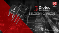
Currently, TO-247 parts are popular as they can be drop-in replacements for some MOSFETs and IGBTS and many types are four-lead to include a Kelvin connection for the gate drive. This helps to overcome the effect of the source lead inductance which otherwise can cause unwanted turn-on with high drain-source di/dt. D2PAK-3L and -7L are also available along with TO-220-3L, TO247 and most recently from UnitedSiC, the surface-mount, low profile DFN8x8 package, optimized for high-frequency operation with its lowest package inductance.
In the future, other SMD packages will be available, most with silver-sinter die-attach for better thermal performance. Multiple SiC die in modules will also become more widely available with perhaps up to 1200V rating for the individual die and 6000V rating or higher using a stacked ‘Supercascode’ arrangement for very high power. These will find use in solid-state transformers, MV-XFC fast chargers, wind energy generation systems, traction, and HVDC generally.
A Glimpse into the Future
Innovation in power applications is rapid and it doesn’t take a crystal ball to see that semiconductor switches need to evolve to keep up with market expectations. There is a clear path however for SiC to follow to meet the demands, with new performance benchmarks. UnitedSiC is currently working on a pipeline of new devices to address ever-wider applications.
Related Content