Facebook
 Google
 GitHub
 Linkedin
What’s Up With Digital Downconverters
Radio architectures can contain more downconversion stages than ever. Here are some tips to keep up.
Radio architectures can contain more downconversion stages than ever. Here are some tips to keep up.
Many current radio architectures contain downconversion stages that translate an RF or microwave frequency band down to an intermediate frequency for baseband processing. Regardless of the end application, whether it is communications, aerospace and defense, or instrumentation, the frequencies of interest are pushing higher into the RF and microwave spectrum. One possible solution to this scenario is to use an increasing number of downconversion stages, such as what is shown in Figure 1. However, another more efficient solution is to utilize an RF ADC with an integrated digital downconverter (DDC) as shown in Figure 2.
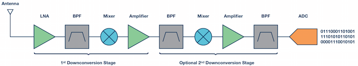
Figure 1. Typical receiver analog signal chain with downconversion stages.
Integrating DDC functionality with an RF ADC eliminates the need for additional analog downconversion stages and allows the spectrum in the RF frequency domain to be directly converted down to baseband for processing. The capability of the RF ADC to process spectrum in the gigahertz frequency domain alleviates the need to perform potentially multiple downconversions in the analog domain. The ability of the DDC allows for tenability of the spectrum as well as filtering via the decimation filtering, which also provides the advantage of improving the dynamic range within the band (increases SNR). Additional discussion on this topic can be found here, “Not Your Grandfather’s ADC,” (PDF) and here, “Gigasample ADCs Promise Direct RF Conversion.” These articles provide some additional discussion on the AD9680 and the AD9625 and their DDC functionality.
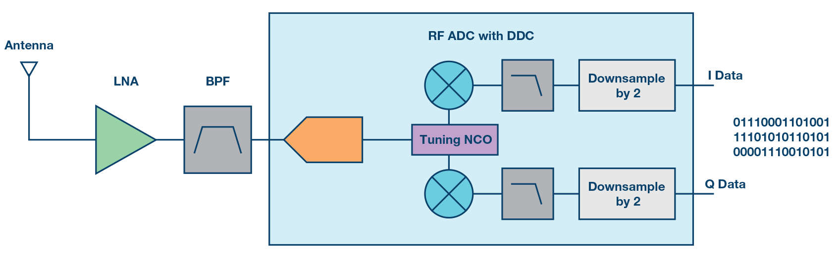
Figure 2. Receiver signal chain using an RF ADC with a DDC.
The primary focus here will be on the DDC functionality that exists in the AD9680 (as well as the AD9690, AD9691, and AD9684). In order to understand DDC functionality and how to analyze the output spectrum when the DDC is employed with an ADC, we will take a look at an example with the AD9680-500. As an aid, the Frequency Folding Tool on the Analog Devices website will be utilized. This simple yet powerful tool can be used to aid in understanding the aliasing effects of an ADC, which is the first step in analyzing the output spectrum in an RF ADC with integrated DDCs such as the AD9680.
In this example, the AD9680-500 is operating with an input clock of 368.64 MHz and an analog input frequency of 270 MHz. First, it is important to understand the setup for the digital processing blocks in the AD9680. The AD9680 will be set to use the digital downconverter (DDC) where the input is real, the output is complex, the numerically controlled oscillator (NCO) tuning frequency is set to 98 MHz, half-band filter 1 (HB1) is enabled, and the 6 dB gain is enabled. Since the output is complex, the complex to real conversion block is disabled. The basic diagram for the DDC is shown below. In order to understand how the input tones are processed, it is important to understand that the signal first passes through the NCO, which shifts the input tones in frequency, then passes through the decimation, optionally through the gain block, and then optionally through the complex to real conversion.
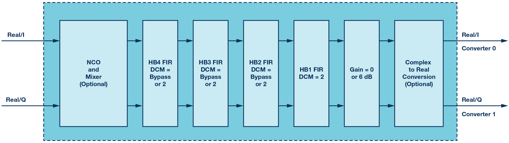
Figure 3. DDC signal processing blocks in the AD9680.
It is important to understand the macro view of the signal flow through the AD9680 as well. The signal enters through the analog inputs, passes through the ADC core, into the DDC, through the JESD204B serializer, and then out through the JESD204B serial output lanes. This is illustrated by the block diagram of the AD9680 shown in Figure 4.
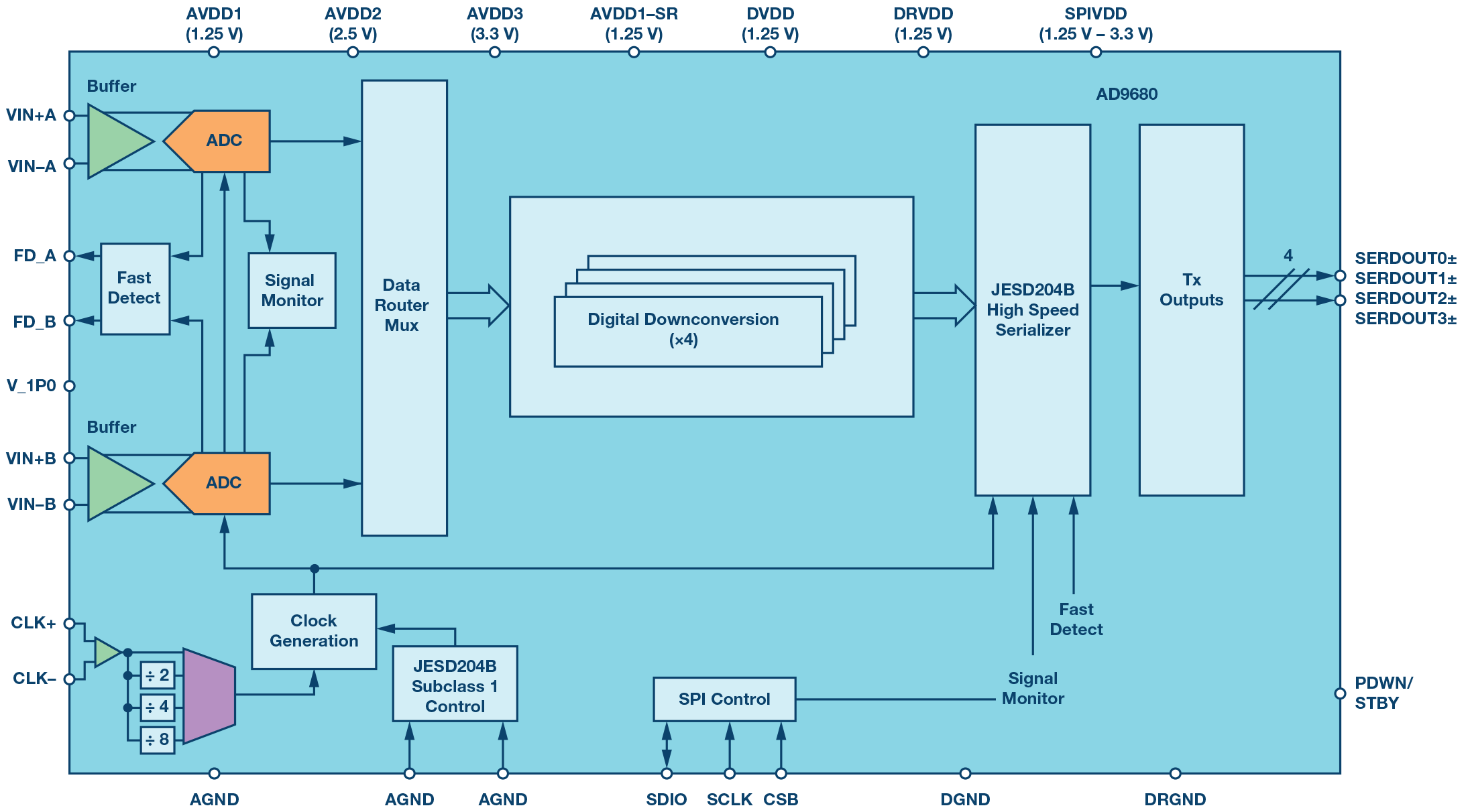
Figure 4. AD9680 block diagram.
With an input sample clock of 368.64 MHz and an analog input frequency of 270 MHz, the input signal will alias into the first Nyquist zone at 98.64 MHz. The second harmonic of the input frequency will alias into the first Nyquist zone at 171.36 MHz while the third harmonic aliases to 72.72 MHz. This is illustrated by the plot of the Frequency Folding Tool in Figure 5.
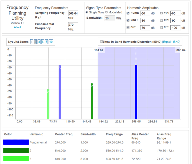
Figure 5. ADC output spectrum illustrated by the Frequency Folding Tool.
The Frequency Folding Tool plot shown in Figure 5 gives the state of the signal at the output of the ADC core before it passes through the DDC in the AD9680. The first processing block that the signal passes through in the AD9680 is the NCO that will shift the spectrum to the left in the frequency domain by 98 MHz (recall our tuning frequency is 98 MHz). This will shift the analog input from 98.64 MHz down to 0.64 MHz, the second harmonic will shift down to 73.36 MHz, and the third harmonic will shift down to –25.28 MHz (recall we are looking at a complex output). This is shown in the FFT plot from Visual Analog in Figure 6 below.
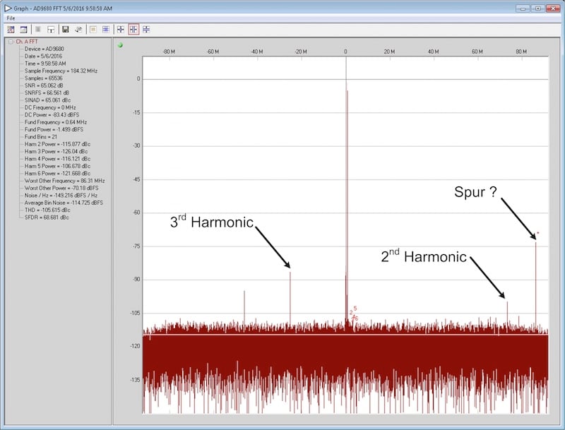
Figure 6. FFT complex output after a DDC with NCO = 98 MHz and decimate by 2.
From the FFT plot in Figure 6, we can see clearly how the NCO has shifted the frequencies that we observed in the Frequency Folding Tool. What is interesting is that we see an unexplained tone in the FFT. However, is this tone really unexplained? The NCO is not subjective and shifts all frequencies. In this case, it has shifted the alias of the fundamental input tone 98 MHz down to 0.64 MHz and shifted the second harmonic to 73.36 MHz and the third harmonic to –25.28 MHz. In addition, yet another tone has been shifted as well and appears at 86.32 MHz. Where did this tone actually come from? Did the signal processing of the DDC or the ADC somehow produce this tone? Well, the answer is no … and yes.
Let’s look at this scenario a bit more closely. The Frequency Folding Tool does not include the dc offset of the ADC. This dc offset results in a tone present at dc (or 0 Hz). The Frequency Folding Tool is assuming an ideal ADC that would have no dc offset. In the actual output of the AD9680, the dc offset tone at 0 Hz is shifted down in frequency to –98 MHz. Due to the complex mixing and decimation, this dc offset tone folds back around into the first Nyquist zone in the real frequency domain. When looking at a complex input signal where a tone shifts into the second Nyquist zone in the negative frequency domain, it will wrap back around into the first Nyquist zone in the real frequency domain. Since we have decimation enabled with a decimation rate equal to two, our decimated Nyquist zone 92.16 MHz wide (recall: fs = 368.64 MHz and the decimated sample rate is 184.32 MHz, which has a Nyquist zone of 92.16 MHz). The dc offset tone is shifted to –98 MHz, which is 5.84 MHz delta from the decimated Nyquist zone boundary at 92.16 MHz. When this tone folds back around into the first Nyquist zone it ends up at the same offset from the Nyquist zone boundary in the real frequency domain, which is 92.16 MHz – 5.84 MHz = 86.32 MHz. This is exactly where we see the tone in the FFT plot above! So technically, the ADC is producing the signal (since it is the dc offset) and the DDC is moving it around just a bit. This is where good frequency planning comes in. Proper frequency planning can help to avoid situations such as this one.
Now that we’ve looked at an example using the NCO and HB1 filter with a decimation rate equal to two, let’s add a little more to the example. Now we will increase the decimation rate in the DDC to see the effects of frequency folding and translating when a higher decimation rate is employed along with frequency tuning with the NCO.
In this example we’ll look at the AD9680-500 operating with an input clock of 491.52 MHz and an analog input frequency of 150.1 MHz. The AD9680 will be set to use the digital downconverter (DDC) with a real input, a complex output, an NCO tuning frequency of 155 MHz, half-band filter 1 (HB1) and half-band filter 2 (HB2) enabled (total decimation rate equals four), and 6 dB gain enabled. Since the output is complex, the complex to real conversion block is disabled. Recall from Figure 3 the basic diagram for the DDC, which gives the signal flow through the DDC. Once again the signal first passes through the NCO, which shifts the input tones in frequency, then passes through the decimation, through the gain block, and, in our case, bypasses the complex to real conversion.
Once again we will use the Frequency Folding Tool to help understand the aliasing effects of the ADC in order to evaluate where the analog input frequency and its harmonics will be located in the frequency domain. In this example we have a real signal, a sample rate of 491.52 MSPS, the decimation rate is set to four, and the output is complex. At the output of the ADC, the signal appears as illustrated below in Figure 7 with the Frequency Folding Tool.
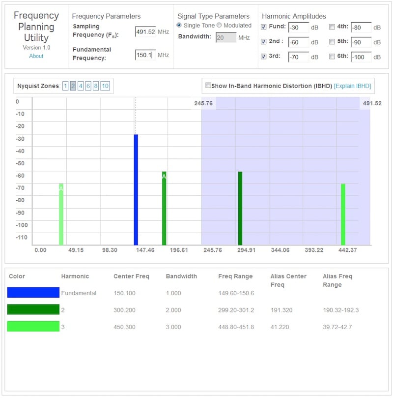 Figure 7. ADC output spectrum illustrated by the Frequency Folding Tool.
With an input sample clock of 491.52 MHz and an analog input frequency of 150.1 MHz, the input signal will reside in the first Nyquist zone. The second harmonic of the input frequency at 300.2 MHz will alias into the first Nyquist zone at 191.32 MHz while the third harmonic at 450.3 MHz aliases into the first Nyquist zone at 41.22 MHz. This is the state of the signal at the output of the ADC before it passes through the DDC.
Now let’s look at how the signal passes through the digital processing blocks inside the DDC. We will look at the signal as it goes through each stage and observe how the NCO shifts the signal and the decimation process subsequently folds the signal. We will maintain the plot in terms of the input sample rate, 491.52 MSPS and the fsterms will be with respect to this sample rate. Let’s observe the general process as shown in Figure 8. The NCO will shift the input signals to the left. Once the signal in the complex (negative frequency) domain shifts beyond –fs/2, it will fold back around into the first Nyquist zone. Next the signal passes through the first decimation filter, HB1, which decimates by two. In the figure, I am showing the decimation process without showing the filter response even though the operations occur together. This is for simplicity. After the first decimation by a factor of two, the spectrum from fs/4 to fs/2 translates into frequencies between –fs/4 and dc. Similarly, the spectrum from –fs/2 to –fs/4 translates into the frequencies between dc and fs/4. The signal now passes through the second decimation filter, HB2, which also decimates by two (the total decimation now is equal to four). The spectrum between fs/8 and fs/4 will now translate to the frequencies between –fs/8 and dc. Similarly, the spectrum between –fs/4 and –fs/8 will translate to the frequencies between dc and fs/8. Although decimation is indicated in the figure the decimation filtering operation is not shown.
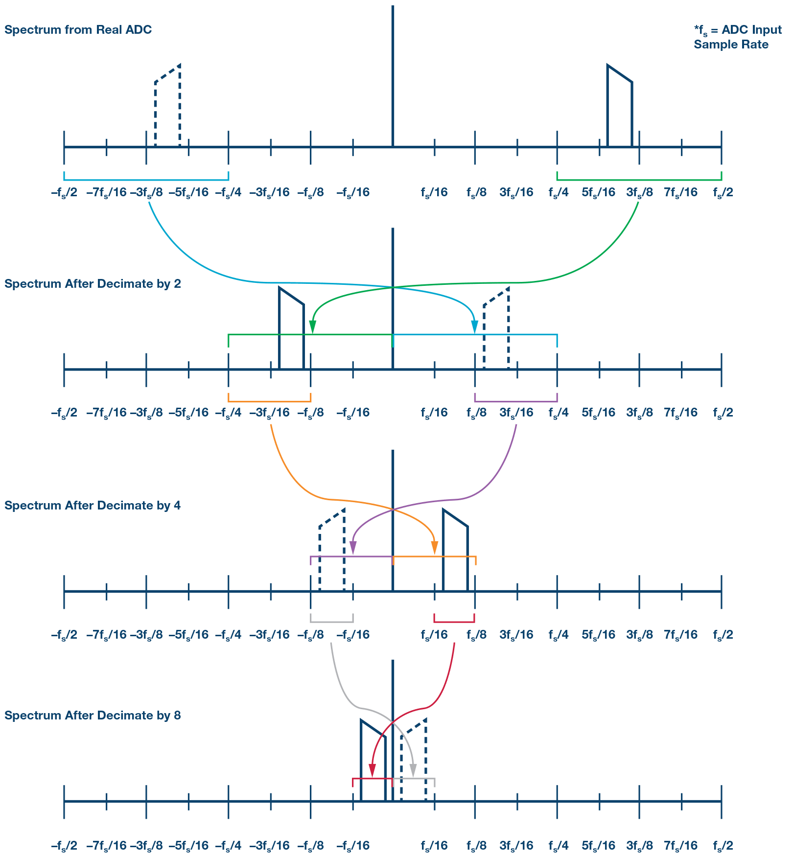
Figure 8. Effects of decimation filters on ADC output spectrum—generic example.
Recall the example previously discussed with an input sample rate of 491.52 MSPS and an input frequency of 150.1 MHz. The NCO frequency is 155 MHz and the decimation rate is equal to four (due to the NCO resolution, the actual NCO frequency is 154.94 MHz). This results in an output sample rate of 122.88 MSPS. Since the AD9680 is configured for complex mixing we will need to include the complex frequency domain in our analysis. Figure 9 shows the frequency translations are quite busy, but with careful study we can work our way through the signal flow.
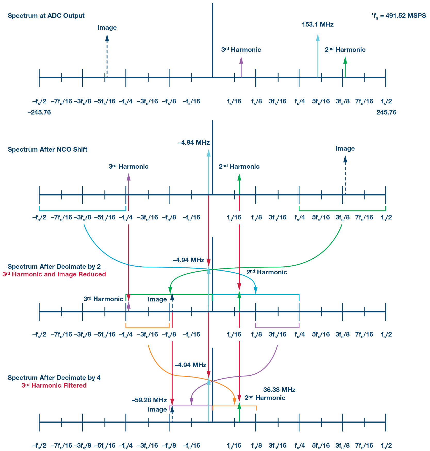
Figure 9. Effects of decimation filters on ADC output spectrum—actual example.
Spectrum after the NCO shift:
- The fundamental frequency shifts from +150.1 MHz down to –4.94 MHz.
- The image of the fundamental shifts from –150.1 MHz and wraps around to 186.48 MHz.
- The second harmonic shifts from 191.32 MHz down to 36.38 MHz.
- The third harmonic shifts from +41.22 MHz down to –113.72 MHz.
Spectrum after decimate by 2:
- The fundamental frequency stays at –4.94 MHz.
- The image of the fundamental translates down to –59.28 MHz and is attenuated by the HB1 decimation filter.
- The second harmonic stays at 36.38 MHz.
- The third harmonic is attenuated significantly by the HB1 decimation filter.
Spectrum after decimate by 4:
- The fundamental stays at –4.94 MHz.
- The image of the fundamental stays at –59.28 MHz.
- The second harmonic stays at –36.38 MHz.
- The third harmonic is filtered and virtually eliminated by the HB2 decimation filter.
Now let’s look at the actual measurement on the AD9680-500. We can see the fundamental resides at –4.94 MHz. The image of the fundamental resides at –59.28 MHz with an amplitude of –67.112 dBFS, which means that the image has been attenuated by approximately 66 dB. The second harmonic resides at 36.38 MHz. Notice that VisualAnalog does not properly find the harmonic frequencies since it does not interpret the NCO frequency and decimation rates.
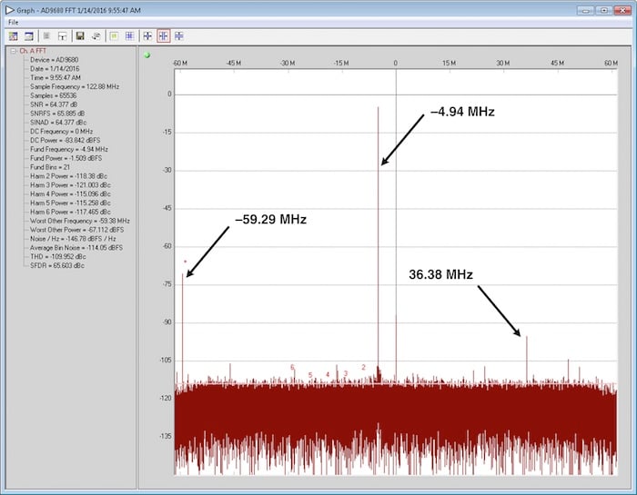
Figure 10. FFT complex output plot of signal after DDC with NCO = 155 MHz and decimate by 4.
From the FFT we can see the output spectrum of the AD9680-500 with the DDC set up for a real input and complex output with an NCO frequency of 155 MHz (actual 154.94 MHz), and a decimation rate equal to four. I encourage you to walk through the signal flow diagram to understand how the spectrum is shifted and translated. I also would encourage you to walk through the examples provided within this article carefully to understand the effects of the DDC on the ADC output spectrum. I recommend printing out Figure 8 and keeping it handy for reference when analyzing the output spectrum of the AD9680, AD9690, AD9691, and AD9684. While supporting these products, I have had many questions related to frequencies that are in the output spectrum of the ADCs that are considered unexplainable. However, once the analysis is done and the signal flow is analyzed through the NCO and the decimation filters, it becomes evident that what were at first considered unexplained spurs in the spectrum are actually just signals residing exactly where they should be. It is my hope that after reading and studying this article you are better equipped to handle questions the next time you are working with an ADC that has integrated DDCs. Stay tuned for part two, where we will continue looking at additional aspects of the DDC operation and also how we can simulate its behavior. We will look at the decimation filter responses due to ADC aliasing, more examples will be provided, and Virtual Eval will be used to observe operation of the DDC in the AD9680 and its effects on the ADC output spectrum.
Further Reading
This article was originally published by Analog Dialogue. Visit their website to view more technical articles.
What's up With Digital Downconverters - Part 2