Facebook
 Google
 GitHub
 Linkedin
Applied Materials and BE Semiconductor Partner to Develop Chip Integration Technology
Applied Materials and BE Semiconductor Industries announce that they are to develop the "industry’s first complete and proven equipment solution for die-based hybrid bonding."
As part of the agreement announced in late October, Applied Materials and BE Semiconductor will work together to develop the industry’s first complete and proven equipment solution for die-based hybrid bonding, an emerging chip-to-chip interconnect technology that enables heterogeneous chip and subsystem designs for applications in artificial intelligence, 5G, and high-performance computing.
The Applied Materials press release explains that the semiconductor industry is moving toward heterogeneous design and chip integration as traditional 2D scaling lags. This shift may be a way to improve performance, power, area/cost, and time-to-market.
It goes on to highlight how the California-based leader in materials engineering solutions has collaborated with BE Semiconductor to form the so-called Hybrid Bonding Center of Excellence (HBCE), which will focus exclusively on the next-generation chip-to-chip bonding technology.
Die-Based Hybrid Bonding
Hybrid bonding connects several chiplets in die form, using direct copper interconnects. The technique enables designers to bring chiplets of various nodes and technologies closer together both physically and electrically so that they’re able to perform as well as, or better than, if they were made on a single monolithic die.
This process is described as an upgrade of traditional chip packaging since it allows for denser chips and shorter interconnect wiring between chiplets.

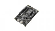
Hybrid bonding uses direct, copper-to-copper interconnects to increase input/output density while shortening interconnect lengths between chiplets. This improves overall performance, power, and cost metrics. Image used courtesy of Applied Materials
The HBCE will be located at Applied Materials’ Advanced Packaging Development Center in Singapore, which is said to be one of the semiconductor industry’s most advanced wafer-level packaging labs.
The center will provide the basic building blocks of heterogeneous integration in a 17,300-square-foot Class 10 cleanroom with full lines of wafer-level packaging equipment. It’ll also provide customers with a platform to accelerate the development and testing of hybrid bonding, including modeling, simulation, and fabrication.
Joint Expertise
Usually, full die-based hybrid bonding equipment calls for a number of different semiconductor manufacturing technologies, including chiplet placement technology.
This is where the value of the partnership between Applied Materials and BE Semiconductor truly lies—Applied Materials' semiconductor process expertise in conjunction with BE Semiconductor’s leading die placement, interconnect, and assembly solutions will provide this broad suite and more for full, unparalleled development of the equipment solution.
“Applied looks forward to working with Besi [BE Semiconductor] to co-optimize our equipment offerings and accelerate advanced heterogeneous integration technology for our customers,” said Nirmalya Maity, Corporate Vice President of Advanced Packaging at Applied Materials.
Applied Materials believes that the collaboration will accelerate the adoption and proliferation of hybrid bonding for 5G, AI, high-performance computing, data storage, and automotive applications.