Facebook
 Google
 GitHub
 Linkedin
Eliyan Talks First Silicon on ‘Most Efficient’ Chiplet Interconnect
Claiming record time for its first silicon, chiplet interconnect specialist Eliyan lays out its case for how its Nulink UCIe interconnect offers advantages over silicon interposer approaches.
All About Circuits recently had the opportunity to discuss the implications of first silicon on Eliyan’s Nulink UCIe compliant chiplet interconnect with co-founder and CEO, Ramin Farjadrad.
The company’s first silicon test chips—just one year after Eliyan’s initial funding—validate their breakthrough in high-performance chiplet interconnect. We last wrote about Eliyan and its UCIe compliant Nulink chiplet interconnect technology at tape-out, back in November 2022.

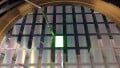
Eliyan’s test setup, including chip and DUT board. Image courtesy of Eliyan
Chiplet architecture SiP is an important part of the race to continue progress in SoC, GPU, and TPU performance and complexity. Traditional system architecture with large monolithic silicon and discrete memory and peripherals don't deliver the performance needed by AI and many of today and tomorrow’s intensive demands. At the same time, single die heterogeneous solutions are essentially becoming too large to effectively manufacture.
More Real Estate Leads to Multiple Advantages
Eliyan, with their Nulink technology, promises significant improvements in chiplet-based device performance. To date, the industry's leading chiplet interconnects require advanced packaging for chiplets and expensive silicon interposers. Nulink interconnects deliver the same or better performance while using conventional chiplet packaging and organic substrates.

Traditional chiplet solution with silicon interposer vs. Eliyan’s Nulink with organic substrate. Image courtesy of Eliyan. (Click image to enlarge)
“One of the big needs today for everyone is being able to get a large enough interposer so they can build bigger and bigger GPUs or TPUs with large memory on it,” said Farjadrad. “This is especially true with generative AI— all of a sudden the demand for on-chip high bandwidth memory exploded. Our test chip validates that we can meet or exceed the bandwidth targets of minimum two and a half terabits per millimeter with super low power consumption.”
Silicon interposers top out in size at about 3,300 mm2, or about 4× the IC die maximum reticule. The Nulink organic substrate can be three times that size while delivering the same or better power efficiency and bandwidth. This leads to lower cost, faster and easier manufacturing, more compute power per package.

Greater surface area allows wider spacing and more chiplets. Image courtesy of Eliyan. (Click image to enlarge)
Increased connectivity reach allows designers to fully utilize the greater real estate. Silicon interposers allow for 2 mm reach while Nulink delivers 20 mm without loss of performance.
“Connectivity reach Is the maximum distance between the ASIC and the memory. In our case, you can go up to 20 mm,” said Farjadrad. “Let's say you can have configurations like this [see diagram above]. With a traditional silicon interposer, you have to limit HBM because you don't have reach, it blocks completely one edge of a chip. But if you have longer reach, as with Nulink, you can stagger them and you can put more HBM on a package.”
The connectivity reach also allows increased spacing of the chiplets. This allows higher clock speeds due to the improved thermal performance and reduced power consumption. More ASICs and more HBM can be combined in the same component than with silicon interposers at a lower cost. You get both more area for chiplets and improved spacing.
Testing and yield is another advantage. The silicon interposer requires the use of microbumps for chiplet to interposer lead connections. The Microbumps limit the ability to fully test the wafer, putting yields at risk.
Nulink’s use of organic substrate mitigates the issue by allowing use of chiplets with standard size bumps, which can be more effectively tested. As such, chiplet fallout can be detected prior to assembly of the SiP, rather than after assembly, increasing yields from 60% to an estimated 90%.
Performance Validation With First Silicon
The test chip, implemented in TSMC’s 5 nm process, was run through its paces in May 2023, and met or exceeded key performance parameters.

Test chip layout. Image courtesy of Eliyan. (Click image to enlarge)
Each interconnect channel has 16 data links plus clock and supports unidirectional modem, meaning each bump can transmit or receive data or bidirectional modem, meaning each bump can transmit and receive simultaneously.
Farjadrad says that the original design target was maximum performance of 28 Gbps/lane for unidirectional and 32 Gbps/lane bidirectional. The test chip proved out to 32 Gbps/lane and 40 Gbps/lane respectively. According to Farjadrad, no one else has achieved these speeds.
“To get this level of performance, every stage has to have enough bandwidth to support it in terms of clock buffer and passing of the signals. In addition, in standard packaging, crosstalk is a big challenge. So we also have interference separation cancellation that enables us to get to this speed.”
Generating this level of performance did not cause a commensurate increase in power requirements. In fact, the power efficiency is at or better than industry standard. The system is comparable in power to other industry solutions.
What Lies Ahead
Today, high-performance processor companies are pressuring TSMC for dedicated fab capacity for silicon interposers. With the supply chain challenges and the time and cost involved in spinning up silicon foundries, a good case could be made that Nulink is arriving just in time to allow that investment to be directed at active devices where it is really needed.