Facebook
 Google
 GitHub
 Linkedin
Exclusive—TSMC Enlightens Us About Its Next Steps in This Q&A
In this article, Gordon posed a set of questions to TSMC about their next steps going forward.
Founded in 1987, TSMC is said to have pioneered the pure-play foundry business, and today ranks as the leading dedicated semiconductor foundry worldwide.
We recently asked the company a set of questions about its next steps. The company’s spokespeople declined to answer our questions, but the ones they did answer offer some interesting insights about semiconductor technology and the industry.
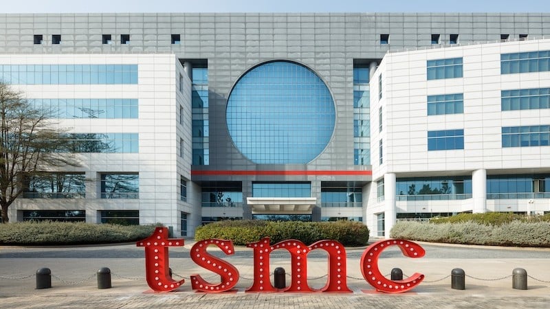
TSMC’s Fab 6
Gordon Feller: What breakthroughs or roadblocks does TSMC foresee in the transition to sub-2nm process technologies?
TSMC: The biggest innovation we are introducing at our 2 nm node is the nanosheet transistor structure, also known as gate-all-around. This is a major step forward, as it is only the second time in our history that we have adopted a completely new transistor structure, and the first time since going from planar to FinFET transistors at the 16 nm node in 2014. Following years of overcoming technical challenges, TSMC is bringing 2 nm technology to volume production by the end of this year.
We will adopt another major innovation at the A16 (1.6nm-class) node with Super Power Rail, our backside power technology. The backside power rail architecture improves logic density and performance by dedicating front-side routing resources to signals, and moving power routing to the back. This structure makes A16 ideal for high-performance computing with complex signal routes and dense power delivery networks.
GF: What long-term technologies—quantum devices, silicon photonics, or alternative materials (e.g., 2D materials, nano-sheet FETs)—are most likely to influence TSMC's post-2nm strategy?
TSMC: TSMC is committed to pushing transistor scaling as far as it can. However, it is not the only way to continue delivering improvements to the performance and functionality of electronic products. We are exploring many paths, such as system-level improvements with 3D IC, design technology co-optimization, and innovative new materials.
In terms of transistor scaling, we have made excellent progress in our research into Complementary Field-Effect Transistors (CFET), where transistors are stacked on top of each other rather than being on the same plane. We have also done significant research into 2D materials that are only one molecule thick, as well as 1D materials such as carbon nanotubes. While these are still in the research stage and not yet on our development roadmap, they show great promise in solving future problems related to shrinking transistors.
Going beyond the transistor, much of our research is related to system-level performance, or how chips within a system interact with each other, and with other systems. This includes silicon photonics, as well as working on heat and power management problems that arise when many chips are packed into the same package.AI demands that processors be able to access massive amounts of data as fast as possible, and much of our work in advanced packaging revolves around creating larger and larger systems that can pack in more memory and computing power.
We already offer System-on-Wafer technology, which is a single system the size of a 12-inch wafer that can potentially offer computing power comparable to a data center server rack, or even an entire server. At the same time, we are already looking beyond the wafer and conducting exploratory research into even larger panel-sized systems.
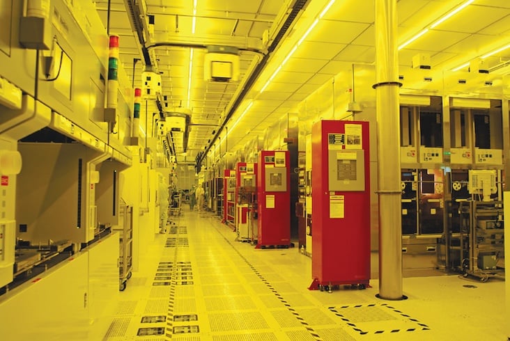
Inside TSMC’s 12-inch wafer fab
GF: How is TSMC evaluating the long-term return profile of its global fab expansion strategy—particularly in the U.S., Japan, and Europe—relative to the rising capital intensity and lower expected yield learning curves outside Taiwan?
TSMC: In terms of yield learning curves, as our Chairman and CEO Dr. C.C. Wei noted in our investor conferences, our first fab in Arizona entered high-volume production in 4Q ‘24, utilizing N4 process technology, with a yield comparable to our fabs in Taiwan. Over time, we’ll leverage our increasing scale in Arizona and work on our operations to improve the cost structure. As it grows, the site will create greater economies of scale, and help foster a more complete semiconductor supply chain ecosystem in the U.S. We will also continue to work closely with our customers and suppliers to manage the impact.
Our Europe and Japan fabs are designed for specialty technologies important to the industries of those regions, and they are not to the same scale as our plans for Arizona. However, we are confident that we can continue to apply the lessons we’ve learned both in Taiwan and overseas.
GF: What scenarios is TSMC modeling for global semiconductor demand in an AI-accelerated economy, and how might those scenarios affect the company’s multi-decade capacity-planning and capex discipline?
TSMC: We continue to observe robust AI-related demand throughout 2025, and we continue to invest for the long-term mega trend driven by this demand. However, we will also continue to focus on the fundamentals of our business, that is technology leadership, manufacturing excellence and customer trust, to further strengthen our competitive position.
Overall, every year, our capex is spent in anticipation of the growth that will follow in future years. Although there is short-term cyclicality in the industry, we believe if the structural long-term demand is there, and the future opportunities are there, we will continue to invest. Our disciplined capex and capacity planning remains based on the long-term market demand profile.
TSMC Declined to Answer Some Questions
We also asked TSMC some additional questions on subjects such as U.S.-China tech competition, shifts in government policies worldwide, and similar topics. In response, TSMC's press team said they prefer to not address geopolitical or trade-oriented questions.
All images used courtesy of TSMC.