Facebook
 Google
 GitHub
 Linkedin
5 Research Breakthroughs Push the Boundaries of Photonic Computing
Recent advances in photonic platforms, memory architectures, and optical switching demonstrate an evolving space for optical computing.
Research teams around the world are accelerating progress in photonic computing, publishing results over the past year that span devices, memory, switching, feature extraction, and high-speed modulation. Recent works cover developments from SiGe photonics and integrated optical memory to single-photon switches, optical diffraction engines, and 400-Gb/s electro-absorption modulators, each aimed at reducing latency or increasing bandwidth in data-intensive systems.
Taken together, these projects offer a view of how optical technologies could support future AI, HPC, and real-time decision-making workloads while remaining compatible with semiconductor manufacturing at scale.
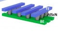
1. IHP Unveils SiGe Photonics Platform With 140 GHz Modulators
IHP has introduced what it calls the first silicon-germanium photonics platform that can support electro-absorption modulators and photodiodes with bandwidths well beyond current silicon-photonics limits, reporting extrapolated 3-dB cut-off frequencies of 140 GHz for its modulators and up to 200 GHz for its fin-photodiodes.

IHP says its new platform overcomes AI bandwidth bottlenecks. Image (modified) used courtesy of IHP
The devices run in the C-band and were fabricated in a single process flow, which the team identifies as a requirement for scaling to beyond-200-Gbaud interconnects. To reach these performance targets, IHP developed a SiGe epitaxy approach using a silicon delta-layer to control the absorption edge while avoiding loading effects in integrated SiGe devices, alongside a compact waveguide-integrated EAM structure and a tunable fin-photodiode design that trades responsivity for bandwidth.
The group validated the platform through a high-speed link experiment using modulators and photodiodes from the same wafer, and it now plans to co-integrate the photonics platform with its BiCMOS technologies to support future high-performance optical links in AI and HPC systems.
2. Integrated Photonic Memory Using Standard Semiconductor Processes
Researchers at the University of Wisconsin-Madison have developed and tested an integrated photonic memory chip built entirely from components already available in commercial silicon photonics foundries, offering a practical path toward scalable optical computing hardware.

The device was designed and tested by Akhilesh Jaiswal, a UW-Madison assistant professor of electrical and computer engineering and PhD student Md Abdullah-Al Kaiser. Image used courtesy of UW-Madison
The device uses a “cross-coupled, differential, regenerative photonic latch” constructed from photodiodes, microring resonators, and optical waveguides to create an optical analog of SRAM, with simulated operating speeds of 20 GHz and read speeds up to 50–60 GHz. Because the design relies solely on standard processes from foundries such as AIM Photonics and GlobalFoundries, it can be manufactured at volume without new materials or fabrication techniques, positioning it for roles in large optical interposers that link processors in data centers and high-performance computing systems.
3. Purdue Researchers Realize Single-Photon Optical Switch
Purdue University researchers have demonstrated a single-photon optical switch that leverages avalanche multiplication to create an exceptionally large nonlinear refractive index, enabling what they describe as a “photonic transistor” operating at single-photon intensities and potentially scalable to hundreds of gigahertz clock rates.
The team adapted the avalanche mechanism used in commercial single-photon avalanche diodes so that a lone photon in a control beam can modulate a much stronger probe beam, bridging quantum-scale effects with macroscopic optical switching. The device works at room temperature and is compatible with CMOS processes, giving it a manufacturing pathway that many quantum-emitter-based nonlinear platforms lack.

Purdue University researchers have demonstrated a “photonic transistor” that operates at single-photon intensities. Image used courtesy of Purdue University
According to the researchers, the switch’s speed already reaches the gigahertz range and could extend far higher with optimized geometries, positioning it for applications ranging from quantum information protocols to classical photonic logic and high-speed optical interconnects. The group is now developing custom SPAD structures tailored for switching rather than detection, aiming to further increase nonlinearity and bring single-photon optical logic closer to practical photonic computing architectures.
4. A 12.5-GHz Optical Feature Extraction Engine
A Tsinghua University team has built a 12.5-GHz optical feature extraction engine that uses integrated diffraction operators and an on-chip data preparation module to achieve sub-250-ps, matrix-vector operations, addressing the latency bottlenecks found in electronic processors used for real-time AI workloads.
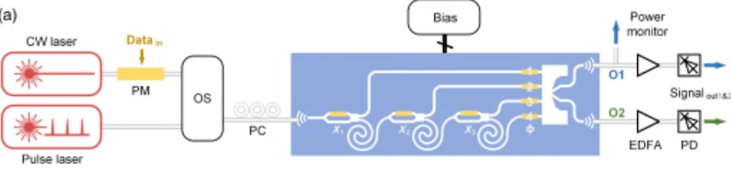
Configuration and functionality validation of the OFE2. Image used courtesy of SPIE Digital Library
The researchers solved the coherence and stability limits of previous optical systems by replacing fiber-based splitters and delay elements with tunable on-chip power splitters, precise delay lines, and a reconfigurable phase array that samples incoming data streams into multiple parallel optical branches. Once prepared, the optical signals propagate through a diffraction operator that steers focused output light based on the input phase arrangement, enabling high-speed feature extraction for tasks such as edge detection and semantic segmentation.
The setup executes a matrix-vector multiplication in 250.5 ps, which is the shortest latency reported for this class of optical computing. The same hardware has been applied to quantitative trading, where the OFE processed time-series market data and generated buy/sell decisions at photonic speeds, demonstrating consistent profitability. The work positions integrated diffraction computing as a practical accelerator for imaging, healthcare, and financial analytics systems that require both low latency and high throughput.
5. Imec Achieves Beyond-110 GHz GeSi Electro-Absorption Modulator
Imec has demonstrated a GeSi electro-absorption modulator on its 300-mm silicon photonics platform that surpasses 110 GHz of bandwidth and supports 400 Gb/s per-lane IM/DD transmission, marking what it identifies as the first C-band GeSi EAM to reach both performance milestones in a manufacturable process.
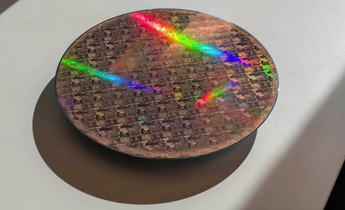
The beyond-110GHz C-band GeSi electro-absorption modulator is fabricated on Imec's 300-mm silicon photonics platform. Image used courtesy of Imec
The modulator targets short-reach optical links inside data centers and AI training clusters, where future architectures expect 400 Gb/s lanes with minimal latency and low power. The device sidesteps the footprint and integration constraints of thin-film LN Mach-Zehnder modulators and the thermal-stability overhead of microring designs by exploiting the Franz-Keldysh effect in germanium-silicon, enabling compact geometry, high speed, and compatibility with wafer-scale CMOS processes.
Imec reports that system-level demonstrations used a PAM-4 IM/DD link to validate the 400-Gb/s net data rate, and emphasizes that measurement equipment—not the device—limited the tested bandwidth to 110 GHz. With higher-frequency instrumentation, the team expects to reveal substantially greater bandwidth headroom and evaluate performance under elevated temperatures typical of data center environments. The modulator is now being made available to partners exploring scale-up interconnects for AI compute clusters.