Facebook
 Google
 GitHub
 Linkedin
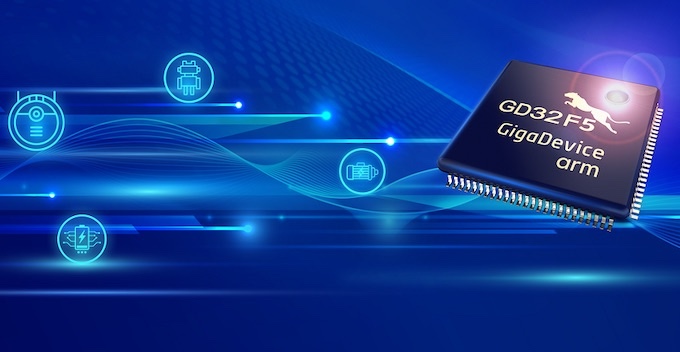
GigaDevice Intros 32-MCU Family Sporting Arm Cortex-M33 Core, 1 MB Flash
The new Arm Cortex-M33 based GD32F503/505 family emphasizes memory flexibility, reliability, and security.
This week, at Embedded World North America in Anaheim CA, GigaDevice announced its new GD32F503/505 series high-performance MCUs. The new family joins GigaDevice’s Arm Cortex-M33 portfolio with the GD32F505 series clocking at 280 MHz and the GD32F503 series at 252 MHz. Variants come with up to 1024 KB (1 MB) flash memory and up to 192 KB SRAM.
The Coretex-M33 leverages Arm-v8 M architecture, and in the GigaDevice implementation comes with a digital signal processor (DSP) hardware accelerator and a single precision floating point unit (FPU).
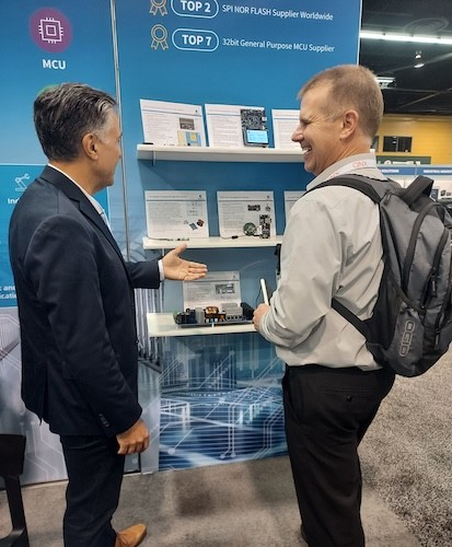
At GigaDevice’s Embedded World NA booth this week, Shahram Mehraban, VP and GM, GigaDevice (left); Dale Wilson, VP of Engineering and Content, All About Circuits (right).
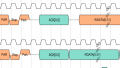
The MCUs are built with a flexible memory architecture that allows developers to scatter load code flash, data flash, and SRAM as needed based on the specific application scenario. Scatter loading allows optimized memory maps to be fed to the tool set at link time.
This gives the programmer greater flexibility in utilizing memory. For example, a real-time interrupt routine, needing the fastest possible response, can be placed into SRAM while non-time critical interrupt routines can reside in flash.
Long Life and High Reliability
The new family sits in the upper half of GigaDevice’s Cortex-M33 portfolio. The flexible memory architecture, solid security feature set, and IEC61508 SIL2 hardware safety integrity level make the processors ideally suited for industrial embedded applications needing reliability and optimized performance.
The new GD32F503/505 family emphasizes memory flexibility, reliability, and security.
Reliability features include enhanced electromagnetic compatibility, high-level ESD protection, (8 kV contact and 15 kV air discharge). Human body model/charge device model (HBM/CDM) immunity at 4000 V / 1000 V holds even after three discharge test runs. GigaDevice estimates a 25-year continuous operation lifespan for the chips.
MCU Key Features
The devices come with a broad peripheral set. Most are memory mapped for easy access and can take advantage of scatter loading in the memory map.
-
Three ADCs sampling at up to 3 Msps (up to 25 channels)
-
Fast comparator (0.65 µS startup time and 24.8 ns full range step propagation delay)
-
One DAC
-
Communication comes through: Three SPI, two I2S, two I2C, three USART, two UART, two CAN-FD, one USBF
-
Timing includes: one 32-bit GP timer, five 16-bit GP timers, two basic timers, two 16-bit PWM timers
-
Three power saving modes
-
2.6 V to 3.6 V operating voltage
-
-40°C to +105°C operating temperature range
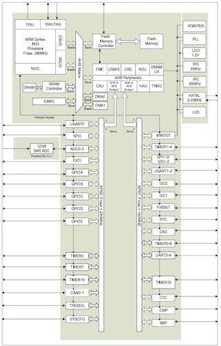
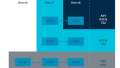
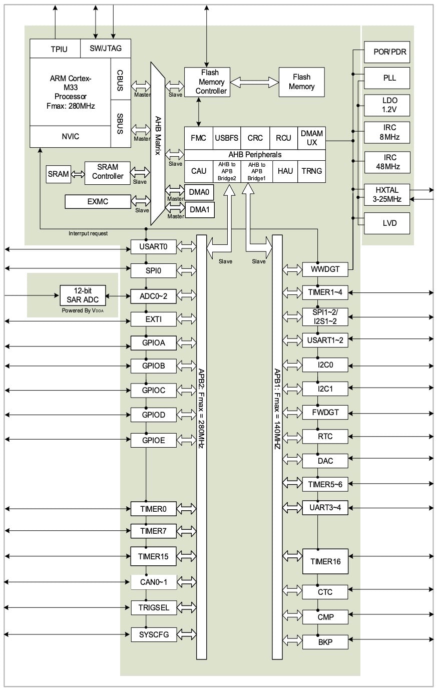
GD32F505 block diagram. (Click image to enlarge)
Device Security
In recent years, MCU vendors have woken up to the need for embedded security. GigaDevice has followed that trend with a solid set of security features in the new MCU family. The GD32F503/505 family comes prepared for today’s embedded threat environment with a comprehensive chip-level security architecture.
-
Secure boot and Secure firmware update (SBFU)
-
User secure storage area with multi-level code and data protection
-
Hardware SHA-256 hash algorithms
-
AES-128/254 encryption algorithms
-
True random number generator (TRNG)
The hardware security architecture includes multi-channel watchdogs, power and clock monitoring, and hardware CRC to ensure the ability to create secure embedded industrial devices. More information can be found in the datasheets for the GD32F503xx and the GD32F505xx.
MCU Ecosystem
GigaDevice offers the chips in multiple QFP, QFN, and BGA packages for implementation flexibility. Development tools include the free GD32 Embedded Builder IDE, GD-LINK debugging and download tools, and the GD32 all-in-one programmers. A variety of third-party Arm tools also support the chip family.
Except where otherwise specified, all images used courtesy of GigaDevice.
Related Content