Facebook
 Google
 GitHub
 Linkedin
IC Breakthroughs: Energy Harvesting, Quantum Computing, and a 96-Core Processor in Six Chiplets
Research institute CEA-Leti is developing techniques to increase the power of semiconductors—with energy-harvesting ICs, a quantum IC that combines quantum dot with digital-analog circuits, and an "active interposer."
According to Moore's law, since the introduction of the first semiconductors, the number of transistors on an integrated circuit has doubled approximately once every 18 months.
However, now that transistors are starting to reach near-atomic sizes, their reduction is becoming increasingly problematic, and as such, this doubling effect is beginning to plateau.
One technology research institute, CEA-Leti, is developing techniques to increase the power of semiconductors.
But what are these new technologies and how will they affect modern electronics?
Responsive Energy Harvesting ICs
Developers are increasingly searching for efficient ways to replace portable power sources that require charging or replacement.
However, such a feat is only possible if power can be extracted from the local environment, like in the instance of a device from the University of Massachusetts Amherst that powers small electronics from moisture in the air.
A more conventional method for energy extraction is using the Peltier effect, which requires a heat differential (such as cold air on a warm wrist), but these are often cumbersome and require heat sinks.
Another method is the use of vibration energy from motion, whereby a cantilever vibrates a piezo element, converting the mechanical energy to electrical energy.
But these systems are problematic because they are often tuned for one frequency of vibration. This means that their efficiency is only maximized when external mechanical energy is of the same frequency.
This is where CEA-Leti’s energy harvesting system comes in.

Diagram of CEA-Leti’s energy-harvesting ICs working within a larger system. Image used courtesy of CEA-Leti
The energy harvesting system converts mechanical energy into electrical energy to power an IC. While similar to a cantilever system, which converts mechanical motion into electrical energy using a piezo effect, the cantilever is electrically tunable, allowing it to match its resonant frequency to the peak frequency of the external mechanical force.
Using an adjustable resonant system increases the harvesting bandwidth by 446% from typical cantilever systems and increases energy efficiency by 94%. The energy needed to control the system is two orders of magnitude lower than what the system harvests; the system requires around 1 µW while the energy harvested is between 100 µW and 1 mW.
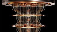
Quantum IC with Quantum Dot with Digital-Analog Circuits on CMOS Chip
While quantum computing will bring some major changes to the field of computation, they are far from becoming commercialized.
Many hurdles, such as low-temperature requirements, make them difficult to put into everyday applications. But one area, in particular, that is problematic is their integration into standard circuitry.
In a study on energy-efficient quantum computing, researchers explain that qubits, which are bits in superposition states, must be kept well away from external sources of energy. This is because any exposure to external energy puts the qubits at risk of collapsing their wavefunction. Such sources of energy can include magnetic field fluctuations, electromagnetic energy, and heat (mechanical vibration).
To make things more complicated, quantum computer circuitry is at some point required to interface with traditional electronic circuitry, such as analog and digital circuits. If these circuits are external to the quantum circuitry, then the issue of space and speed become an issue; remote circuitry takes more room, and the distance reduces the speed at which information can be accessed.

According to CEA-Leti, the "quantum integrated circuit is a proof-of-concept circuit merging microelectronics benchmarks and quantum dots operating at a sub-Kelvin temperature within a limited power budget." Image used courtesy of CEA-Leti
To address these issues, CEA-Leti has developed a quantum computing technology that combines qubits with traditional digital and analog circuitry on the same piece of silicon using standard manufacturing techniques.
The 28 nm FD-SOI process combines nA current-sensing analog circuitry, buffers, multiplexers, oscillators, and signal amplifiers with an on-chip double quantum dot whose operation is not affected—even when using the traditional circuitry at digital frequencies up to 7 GHz and analog frequencies up to 3 GHz.
The IC, which operates at 110 mK, is able to provide nA current-sensing while operating on a power budget to prevent interference with the quantum dots, which is 40 times lower than competing technologies.
Active Interposer and 3D Stacked Chiplets
As the number of transistors on a chip increases, the chances of one failing also increases, thus decreasing the yield of wafers. One workaround is to make chips smaller and include fewer transistors while also connecting multiple chips together, thus increasing the overall transistor count.
However, PCBs have issues with connecting multiple dies together. These issues may involve limited bandwidth and the inability to integrate other active circuitry required by the dies, such as power regulation.
CEA-Leti has made a breakthrough in IC technology with its active interposer layer and 3D stacked chips.

Diagram of the active interposer, its package, and 3D integration cross-section. Image used courtesy of CEA-Leti
Namely, the team has developed a 96-core processor on six chiplets, 3D stacked on an active interposer.
Just like the PCB topology, CEA-Leti uses a layer with metal interconnects that connect different dies on a single base. But unlike a PCB, the interconnection layer is a piece of semiconductor only 100 μm thick.
What makes the interposer more impressive is that it is active. It also has integrated circuitry, including transistors. Therefore, the interposer can integrate power regulators, multiplexers, and digital processors, meaning that the dies directly attached to the imposers operate at high-speeds. They also have all their needed handling circuitry next to them.
The use of the active imposer also means that smaller ICs with reduced transistor counts can be combined to produce complex circuitry. This improves wafer yields, reduces their overall cost, and expands their capabilities.
What Is the Future of This Technology?
These three technologies coming out of CEA-Leti give us a glimpse into a future where ICs may generate their own power or even be able to integrate quantum circuitry.
The energy harvesting technology may struggle to find its way into modern designs because most portable applications require relatively large amounts of power (compared to 1 mW) and these devices are often stationary.
The use of quantum circuitry with traditional construction techniques means that quantum security (which may become essential) can be integrated into everyday devices such as smartphones, tablets, and computers. Until quantum computing becomes commercial, though, this technology will likely remain niche.
Technologies such as the active imposer may be the first technology of the three discussed here to become widespread as it easily solves modern transistor reduction-related issues.
Is there a specific functionality you can't seem to find in an IC? What limitations do you feel are keeping researchers from making your "dream" IC breakthrough? Share your thoughts in the comments below.