Facebook
 Google
 GitHub
 Linkedin
ISSCC 2025: Intel Propels Chiplet Interconnect Speed and Flexibility
The company demonstrated configurable, bandwidth-scalable heterogenous 2.5D interfaces across 20 chiplets from two foundries.
At ISSCC 2025, Intel scientists presented a paper outlining a configurable silicon substrate based on a standard chiplet interface compatible across chiplet types and manufacturers. The paper also proposes a standard interface template for chiplet design with on-chiplet routers for dynamically changing system routing during runtime.
One of the key goals of the new architecture is to remove bandwidth bottlenecks in high-demand AI applications. The proposed solution enhances design flexibility by standardizing the chiplet interface and creating a “mix and match” compatible host for chiplets of various types from different manufacturers.
It also increases operational efficiency and removes bottlenecks by adapting chiplet-to-chiplet routing in real time to bypass unused chiplets. For example, a CPU core not being used in a specific AI inferencing application can be dynamically removed from a pathway between a graphics processing unit (GPU) and a memory chip. This will reduce transfer bottlenecks during data-intensive operations. The CPU code can be routed back in when needed for other operations.
Taking 2.5D Chiplet Architecture Farther
Chiplet architecture has taken the front row in designing and constructing complex processing units. It can significantly improve processing power without the yield risk of making chips out of larger areas of silicon. A silicon interposer acts like a high-speed communications path between chiplets.
Chiplet-on-interposer construction, known as 2.5D architecture, disaggregates functionality into smaller chiplets. Processor vendors can easily mix and match when adding in high-bandwidth memory, different types of processing cores, and high-speed data interfaces.
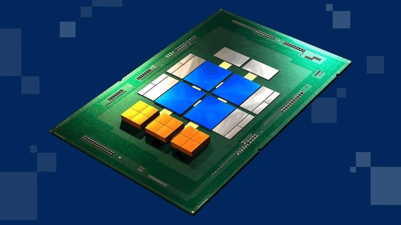
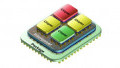
Intel 2.5D chiplet architecture.
The new Intel architecture pushes 2.5D further by standardizing parts of the interface to enable multi-manufacturer chiplet integration. It further increases design flexibility by integrating an Advanced eXtensible Interface (AXI)-based, die-to-die router network, increasing chiplet capacity on the substrate. The architecture can accommodate multiple combinations of chiplets on the same substrate. Developers can perform configurations to accommodate the specific combination of chiplets at assembly time.
Chiplet Interconnect Standardization
In Intel's ISSCC paper, the company proposes an even more advanced 2.5D chiplet solution. The methodology proposes a set of standards to allow interoperability and assembly-time configuration of chiplet systems. Chiplets of different types, such as CPUs, GPUs, and memory, would have a common interface. A passive silicon substrate has lands for multiple chiplets; 20 were used in Intel's experiment. Each chiplet has a standard set of interface bumps. The chiplets have a reconfigurable router circuit that can take the chiplet in or out of the circuit based on demand.
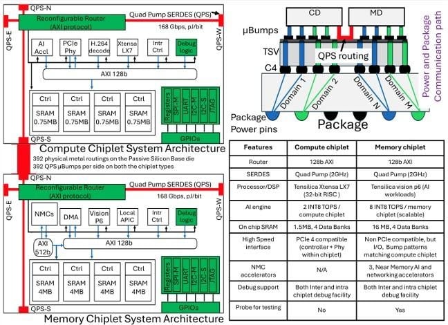
Active chiplet architecture.
The figure above illustrates one memory chiplet (bottom left) and one compute chiplet (top left). The common communications and AXI routers are highlighted in green. The AXI router circuitry controls whether the chiplet is active on the bus or not. When a chiplet is inactive, the AXI system can optimize the route signals between chiplets for higher performance. Unused chiplets essentially get out of the way until they are needed again, at which time the AXI routes them back in.
Standard Chiplet Template
The paper proposes a standard chiplet template. Current chiplet designs place the interface based on internal layout expediency and overall system design constraints. The Intel proposal puts forward a standard template that would improve interoperability with minimal layout compromise.
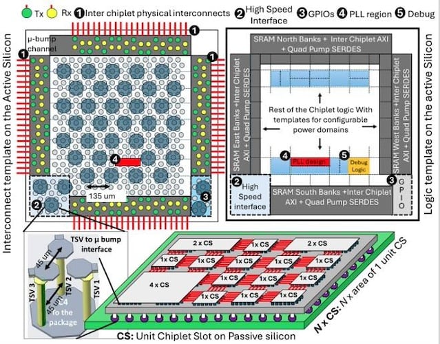
Chiplet standard template.
In the figure above, the microchannel bumps for chip interconnects are located around the periphery of the chip. High-speed interfaces and GPIO are placed in fixed locations. The center area under the chiplet is reserved for thru-silicon-vias (TSVs) to connect to the package substrate and route power and ground.
Verifying Performance
The Intel team created a test scenario using 20 chiplets from two different manufacturers. The test setup included a Tensilica LX7 processor, an H.264 media decoder, a PCIe4 PHY, and a controller for external communication with the host processor. It also included an AI accelerator with 2 INT8 TOPS, a custom debug logic engine, a 3-MB SRAM subsystem, and register files (RF) for chiplet and system configuration (vi) test logic and GPIOs.
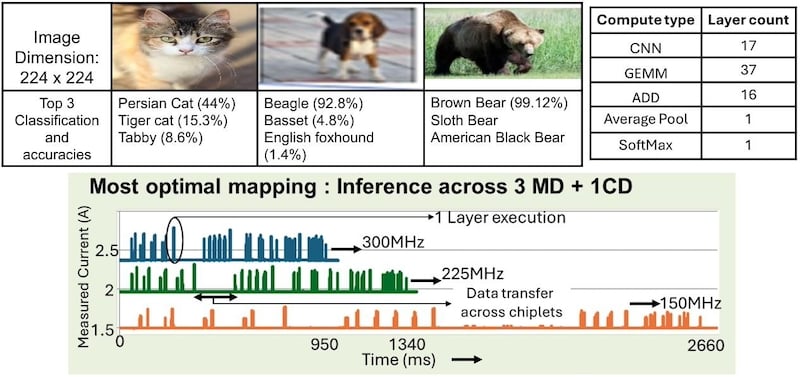
ResNet50 verification test with current charting.
The standardized debug systems in the template included open-drain I/Os with multi-leader capability. This capability allowed debug on individual chiplets without requiring a scan chain to go through the entire system for each debug. The system successfully performed the AI test ResNet50, with the ImageNet dataset across three different memory and compute chiplet configurations. The test's success verified that performance was not compromised by configurability overhead or template standardization.
Faster Time to Market, Better Performance
Intel's end goal with this research is to develop a higher-performing and more versatile chiplet architecture for high-performance chips. Such an architecture could underlie next-generation system-on-chip (SoC) processors, AI processors, and other maximum-performance processing units.
By utilizing real-time routing to remove inactive chiplets, the architecture will reduce bottlenecks commonly associated with chiplet systems. With the flexibility that comes with configuring at assembly time, Intel and others following the proposed standards will be able to deliver a wider variety of customized and more targeted application chips by mixing and matching the most appropriate set of memory, communications, and processing chiplets.
All images used courtesy of Intel.