Facebook
 Google
 GitHub
 Linkedin
Memory Startup Pitches Space-Efficient ‘GCRAM’ as SRAM Drop-In
Fresh from a $17.5M Series A, RAAAM’s novel embedded memory tech aims to reshape SoC design, pushing beyond the SRAM-DRAM tradeoff.
In the race for faster, more efficient memory in edge devices, SRAM remains a performance king, but a silicon hog. DRAM offers density but fails on latency and integration. Now, a startup spun out of Hebrew University, RAAAM Memory Technologies, believes it’s cracked this long-standing dichotomy with its Gain-Cell Random Access Memory (GCRAM) architecture. RAAAM claims this technology is a drop-in SRAM alternative offering near-equivalent latency at significantly smaller area and lower power.
Fresh off a $17.5 million Series A led by NXP Semiconductors and joined by industry veterans, including Fusion Fund, RAAAM is preparing to bring its IP to commercial silicon. The funding will accelerate GCRAM’s transition from foundry-compatible prototypes to mass production at leading nodes, including 16-nm FinFETs.
Following the oversubscribed funding round, RAAAM will fully qualify its patented on-chip memory technology on the leading-edge process nodes of several foundries.
From Academic Foundations to Foundry Silicon
RAAAM’s origin story traces back to 2021, when a team of four co-founders began developing novel memory architectures rooted in academic research on DRAM and SRAM hybridization.
Unlike many memory startups that require new materials and novel devices, RAAAM pursued a fully CMOS-compatible architecture using standard logic process flows. That decision lowered the barrier for IP licensing and eased integration with existing design flows, an approach that caught the eye of NXP, which is now working closely with RAAAM on deployment in real SoCs.
The startup’s early validation came in the form of a 16-nm test chip fabricated through TSMC, showing working silicon that met projected latency and density targets. That chip demonstrated RAAAM’s capability to design, implement, and verify functional silicon on a leading foundry node.
Gain-Cell Random Access Memory Finds a Happy Medium
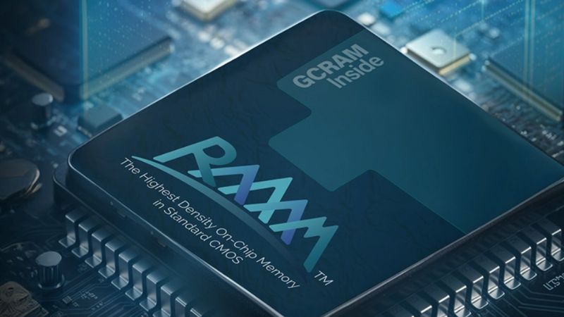
At the heart of RAAAM’s value proposition is Gain-Cell Random Access Memory (GCRAM), a memory array architecture that combines aspects of DRAM and SRAM while avoiding the scaling challenges of both. Traditional SRAM cells are fast but large and volatile. DRAM is denser but requires complex refresh and controller infrastructure, and it’s rarely embedded.
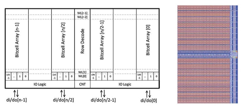
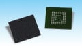
RAAAM’s drop-in SRAM replacement, GCRAM.
GCRAM takes a middle path. It uses a 3T cell structure with no need for external capacitors or refresh controllers. Its latency and endurance are close to SRAM, but its density is significantly better: RAAAM claims up to 4x improvement in memory density compared to 6T SRAM, depending on implementation.
What distinguishes GCRAM from legacy gain-cell RAMs is RAAAM’s proprietary circuit techniques to improve retention time, reduce leakage, and manage write disturb effects. These innovations are what elevate the architecture from a niche memory to a general-purpose, SRAM-replacement candidate. Importantly, it’s designed to fit into standard digital flows and can be delivered as a hard macro or RTL-compatible IP block.
What Markets Does GCRAM Target?
RAAAM’s 16-nm test silicon has validated GCRAM’s operation across PVT corners, showing performance in high-temperature and low-voltage regimes suitable for automotive-grade applications. On a per-bit basis, it shows up to 70% reduction in area and 90% reduction in leakage power compared to SRAM, depending on the use case.
The market opportunity for embedded memory alternatives is vast. SRAM occupies ~70% of the die area in many modern SoCs, especially for AI/ML inference chips, edge processors, and automotive MCUs. Any technology that can reduce this footprint without compromising latency or power offers compelling system-level value.
RAAAM is targeting exactly these high-growth segments. Edge AI accelerators are memory-bound, with workloads that benefit from fast local scratchpad memory but suffer under large SRAM area budgets. With more in-vehicle intelligence (including ADAS and domain controllers) and safety demands, large local memory banks must be robust, power-efficient, and scalable.
What’s Next for RAAAM?
The Series A, led by NXP, brings alignment with major SoC vendors who see real integration potential. NXP, which builds MCUs and domain controllers for automotive and industrial markets, is a logical first mover for embedded memory adoption. With area savings directly translating to BOM reduction and cost efficiencies in these margin-sensitive domains, GCRAM offers a clear economic case. RAAAM has also received grant support from the European Innovation Council.
Next steps for RAAAM include scaling its IP to additional process nodes while expanding its offering into compiler-integrated cache memories and specialty blocks like CAMs and scratchpads. Work is also underway to bring GCRAM into chiplet-friendly architectures, positioning it as a modular memory tile for disaggregated computing.
All images used courtesy of RAAAM Memory Technologies.