Facebook
 Google
 GitHub
 Linkedin
Quantum-Dot Transistors: A Potential Alternative to Flexible Electronics?
Researchers at Los Alamos National Laboratory in collaboration with the University of California Irvine have created transistors out of quantum dots to create functional logic circuits.
In a study published in the journal Nature in mid-October, researchers from Los Alamos National Laboratory and the University of California Irvine explain how quantum dot technology provides an opportunity to combine the advantages of well-understood inorganic semiconductors with the chemical processability of molecular systems, presenting a functional CMOS circuit.
This innovation, the researchers say, promises a cheaper and manufacturing-friendly approach to complicated electronic devices that can be fabricated via simple solution-based techniques. But what exactly are quantum dots and what makes this research significant?
What are Quantum Dots?
A quantum dot is a human-made nanoscale crystal that can transport electrons due to quantum effects. One of the most valuable noticeable effects of quantum dots is their photoluminescent properties, enabling them to emit light of various colors when exposed to UV light, making them useful in a variety of applications.

Depiction of quantum dot sizes and corresponding emitted light. Image used courtesy of Nano Werk
It’s also possible to get semiconductor quantum dots that exhibit semiconductive properties, and it’s these that are required for creating quantum dot transistors like that demonstrated by the Los Alamos National Laboratory (LANL) and the University of California, Irvine (UC Irvine) researchers in this study.
Quantum Dot Transistors
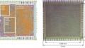
Microelectronics has long since relied on high purity silicon processed in clean-room environments, however, silicon-based microelectronics has faced several challenges recently from technologies that can be inexpensively fabricated using chemical processes outside of such environments. Colloidal semiconductor nanoparticles are one such example which, due to their small size and properties controlled by quantum mechanics, are referred to as colloidal quantum dots.
Colloidal quantum dots consist of a semiconductor core surrounded by organic molecules.
This hybrid nature means that they combine the advantages of semiconductors with the versatility of molecular systems. As such, they’re useful for realizing new types of flexible electronic circuits that could be printed onto any surface, potentially bringing benefits to key fields like consumer electronics, security, and medical technology.
“Potential applications of the new approach to electronic devices based on non-toxic quantum dots include printable circuits, flexible displays, lab-on-a-chip diagnostics, wearable devices, medical testing, smart implants, and biometrics,” said Victor Klimov, a physicist specializing in semiconductor nanocrystals at LANL and lead author of the paper.

By depositing gold and indium contacts, the LANL-UC Irvine team created two types of quantum dot transistors on the same substrate. Image used courtesy of Los Alamos National Laboratory/University of California, Irvine
Although the first quantum dot transistors were demonstrated around two decades ago, integrating complementary n- and p-type devices within the same quantum dot layer has been a challenge difficult for researchers to overcome.
While other research efforts have explored the use of nanocrystals based on lead and cadmium to overcome this challenge, these are toxic heavy metals which would limit the practical utility of demonstrated devices.
Addressing the Toxicity Problem
By using copper indium selenide (CuInSe2), however, the LANL-UC Irvine research team demonstrated that quantum dots devoid of heavy metals could address the toxicity problem, as well as achieve straightforward integration of n- and p-transistors in the same quantum dot layer.

Diagram of the bottom-gate, bottom-contact CQD FET. Image used courtesy of Nature
The innovation presented in this study allows the researchers to define n- and p-type transistors by applying gold and indium metal contacts respectively. The devices were completed by depositing a common quantum dot layer on top of the pre-patterned contacts. To demonstrate the practical utility of their approach, the researchers created functional CMOS circuits that were able to perform logical operations.
“This approach permits straightforward integration of an arbitrary number of complementary p- and n-type transistors into the same quantum dot layer prepared as a continuous, un-patterned film via standard spin-coating,” said Klimov.
Related Content