Facebook
 Google
 GitHub
 Linkedin
Semiconductor Fab Shakeups Signal Application-Focused Plans Ahead
Major players are reshaping the semiconductor map: TSMC exits GaN, Infineon scales it up, GlobalFoundries goes vertical with MIPS, and TI backs U.S. fabs with $60B.
In just the past few weeks, four major players—TSMC, Infineon, GlobalFoundries, and Texas Instruments—have made high-stakes announcements that, taken together, chart a course for the next decade of compute and power.
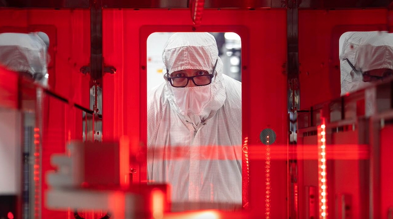
An employee oversees the transfer of a wafer at TI's 300-mm SM1 fab in Sherman, Texas. Image used courtesy of Texas Instruments
GaN is out at TSMC but scaling fast at Infineon. GlobalFoundries (GF) is absorbing MIPS to deliver custom RISC-V AI platforms. And TI is doubling down on American-made analog chips with the largest U.S. fab investment in history.
TSMC Exits GaN Foundry
TSMC will wind down its GaN wafer foundry business by July 2027, citing unsustainable price pressure from Chinese rivals and a realignment toward advanced packaging and AI-focused silicon. GaN makes up a minor portion of TSMC’s output—just 3,000–4,000 wafers per month—but growing subsidies and scale in China have eroded its profitability. Instead, TSMC will repurpose its Hsinchu Fab 5 for CoWoS, WoW, and WLSI technologies to meet surging AI demand, where margins are higher and differentiation is stronger.
This move marks a shift away from niche compound semiconductors toward scale-intensive platforms better aligned with TSMC’s core strengths. It also reshapes the market: Navitas will migrate production to PSMC starting in 2026, while players like Infineon are stepping in with 300-mm GaN production. For design engineers, the impact will be gradual but significant, and they should expect a tighter, more regionalized GaN supply chain and growing consolidation in compound semiconductor foundry services by 2027.
Infineon’s GaN Strategy Scales Up as Others Exit
Infineon’s move to 300-mm GaN wafer manufacturing is a calculated response to both market demand and competitive openings. With TSMC set to exit GaN foundry services by 2027 and Chinese price competition squeezing margins, Infineon is doubling down on its integrated device manufacturer model, controlling design through production in-house.
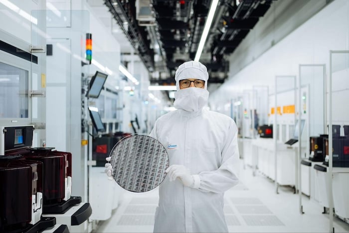
An Infineon lab worker holds a 300-millimeter GaN wafer. Image used courtesy of Infineon
By leveraging its existing 300-mm silicon fabs in Austria, Infineon not only accelerates GaN scaling but reduces costs and ensures design flexibility, positioning itself as a key supplier across power-hungry sectors like AI systems, EVs, robotics, and solar inverters.
This shift reflects broader technology trends. GaN’s high efficiency, small footprint, and fast switching capabilities are increasingly favored over silicon in next-gen power electronics. With customer samples expected by Q4 2025 and over 40 GaN products launched in the past year, engineers could begin seeing real-world impacts in designs as early as 2026.
GlobalFoundries Acquires MIPs
GlobalFoundries' acquisition of MIPS marks a calculated push into the growing edge AI and real-time computing market. By integrating MIPS’ RISC-V–based Atlas processor IP with its differentiated manufacturing platforms, GF aims to offer vertically integrated solutions spanning from silicon to software. This is an obvious response to customer demand for AI-capable, low-latency compute in automotive, industrial, and datacenter applications, where open architectures and physical AI are gaining traction.
The deal also signals a shift away from reliance on third-party processor IP. By owning a scalable, royalty-free compute stack, GF can tailor AI accelerators and real-time cores to specific workloads. With MIPS continuing to operate as a standalone business, engineers can expect gradual integration, with the effects likely to surface in design cycles starting in 2026. The move positions GF as not just a foundry, but a full-stack compute partner in a fragmented semiconductor market.
Texas Instruments Pours $60 Billion Into U.S. Production
Texas Instruments has announced a historic $60 billion investment across seven U.S. fabs, demonstrating a decisive commitment to reshoring foundational chip production, particularly analog and embedded processors essential to everything from EVs to AI data centers.
By focusing on mature 300-mm nodes and vertical integration, TI sidesteps the high-risk bleeding edge to build a stable, scalable supply for partners like Apple, Ford, Nvidia, and SpaceX. The move reinforces U.S. semiconductor sovereignty while addressing long-term national security and industrial capacity goals.
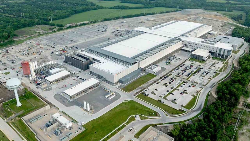
Texas Instruments’ new 300-mm semiconductor fabs in Sherman, Texas, SM1 and SM2. Image used courtesy of Texas Instruments
Engineers will begin seeing real impacts in 2025 as Sherman’s SM1 fab starts output, with others following through 2030. TI’s approach prioritizes cost efficiency (40% lower than 200-mm fabs), lifecycle longevity, and environmental sustainability, all wrapped into a made-in-America strategy backed by CHIPS Act funding. For the engineering community, this should mean more domestic sourcing options and a reliable foundation for the next wave of intelligent, electrified systems.
These announcements indicate that the age of one-size-fits-all silicon is giving way to more focused, regionally anchored semiconductor markets, where efficiency, integration, and application-specific design take the lead.
Related Content