Facebook
 Google
 GitHub
 Linkedin
STMicroelectronics Research Development Project Results in Efficient Semiconductor Laser for Silicon Chips
For a long time, researchers have been looking for a way to integrate lasers directly into silicon chips. This is because transistors, which currently work electrically, can transmit data faster by using light.
Now, researchers from Forschungszentrum Jülich, in conjunction with the Centre de Nanosciences et de Nanotechnologies (C2N) in Paris and the French company STMicroelectronics, as well as CEA-LETI Grenoble, have developed a compatible semiconductor laser made of germanium and tin, with an efficiency that is comparable with conventional GaAs semiconductor lasers on Si.

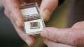
Production of high-concentration germanium-tin compound used in the CMOS production process. Image used courtesy of Forschungszentrum Jülich
Pure Silicon Is Unsuitable as a Laser Material
Optical data transfer enables much higher data rates and ranges than current electronic processes while using less energy. Consequently, data centers default to optical fiber whenever cables exceed a length of one meter.
In the future, demand for optic solutions with distances shorter than this will grow due to increasing requirements, for example, chip-to-chip data transfer. This applies more to areas in emerging tech such as artificial intelligence (AI) systems where a large amount of data must be transferred within a large network for training algorithms.
"The most crucial missing component is a cheap laser, which is necessary to achieve high data rates. An electrically pumped laser compatible with the silicon-based CMOS technology would be ideal," explains Prof. Detlev Grützmacher, director at Forschungszentrum Jülich's Peter Grünberg Institute (PGI-9). "Such a laser could then simply be shaped during the chip manufacturing process since the entire chip production is ultimately based on this technology."
However, pure silicon is unsuitable as a laser material because it is an indirect semiconductor. Currently, different materials are used to manufacture lasers—III-V compound semiconductors. "Their crystal lattice, however, has a completely different structure than that of silicon, which is a group IV element. Laser components are currently manufactured externally and must be integrated subsequently, which makes the technology expensive," explains Grützmacher.

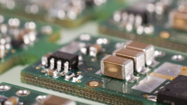
A graphic depicting the pumping process for a laser's (short for light amplification by stimulated emission of radiation) energy being fed into the active medium and resulting in laser radiation. Image used courtesy of Forschungszentrum Jülich
A Laser Based on Germanium and Tin
In contrast to this, the new laser can be manufactured during the CMOS production process. And, like silicon, it is based on two group four elements. However, a high tin content decreases laser efficiency, consequently requiring a relatively high pumping power at around 100-300 kW/cm2 at 12 to 14% tin. Thus, the research team tried to reduce the concentration of tin and compensate this by additionally stressing the material, which improves the optical properties.
For the new laser, the researchers reduced the tin content to around 5%. This decreased the pumping power to 0.8 kW/cm2 which produces little waste heat, allowing it to be operated as a continuous-wave laser.
"These values demonstrate that a germanium-tin laser is technologically feasible and that its efficiency matches that of conventional III-V semiconductor lasers grown on Si. This also brings much closer to an electrical pumped laser for industrial-application that works at room temperature," explained Grützmacher
Potential applications for the laser range from infrared and night-vision systems to gas sensors for environmental monitoring.
Related Content