Facebook
 Google
 GitHub
 Linkedin
The Rise of Toshiba’s New 3D NAND Flash Memory
Get an update on Toshiba's advances in 3D flash memory, just in time for Flash Memory Summit.
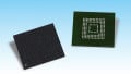
Toshiba has released new 3D NAND technology for high-density memory storage. AAC interviewed Toshiba's Scott Nelson, Senior VP of the Memory Business Unit, and Doug Wong, senior member of the technical team, about what's new and why these advances are important.
In the past two months, Toshiba has made a series of announcements regarding their advancements in 3D flash memory. In late June came the news of their 4th generation memory, which increased from the previous generation's 64 layers to 96, along with the announcement of 4-bit-per-cell technology. Shortly after, TSV (Through Silicon Via) technology was announced, allowing for TLC (triple-level cell) technology.
AAC recently got to speak with Scott Nelson and Doug Wong from Toshiba's memory team. They chatted with us about why 3D memory is so important, how they developed this new technology, and why silicon is still king in the memory industry.

All images used courtesy of Toshiba unless otherwise indicated.
AAC: What can you tell us about QLC technology?
Scott: The QLC is what we call the quad-level cell. That means that we're doing 4 bits per cell. It's kind of interesting because that's never been really in production in the past.
Even though there were demonstrator projects probably more than 10 years ago, it didn't make sense in floating gate to really develop QLC because regular die shrinks were certainly enough to achieve that cost improvement that QLC promised. But the fact that we can now readily implement the QLC technology in 3D allows us to have even lower cost per bit by storing four bits of data in one memory cell. That just wasn't so practical in the past. But that's a technology development that is kind of enabled by the development of BiCS flash.
AAC: Can you tell us what the term "BiCS" means?
Scott: It stands for "bit column stacked". There's definitely some history behind that. When Toshiba first introduced 3D NAND back in 2007 in a research paper, they used the acronym "BiCS". In that paper, they called it "bit cost scalable". There's actually still a lot on the web that says "bit cost scalable". But ultimately we decided BiCS stood for "bit column stacked" to indicate the 3D NAND technology.

AAC: Why are these developments in 3D flash memory so important?
Scott: Let me just start with the fact that the overall storage demand continues to grow, along with the need for higher-density and cost-effective storage. Floating gate, as you may know, ran its time. It's essentially hit the wall. So, in order for the memory technology to continue evolving, we found it was necessary to use the z-axis and so that was the birth of the 3D technology.
Way back when, Toshiba first introduced the concept of BiCS to IEEE about 3D technology. So what does that mean? Really, it's just about your ability to increase the density per chip. Take our 4th-generation 3D memory, which is 96-layer—when you stack 16 chips in a package, you get a one terabyte package. That's pretty significant when you consider how many placements you want to put on an SSD and really scale up the density.
You might say "So what? Why is that so important?" But we all know that enterprise data centers are becoming more and more pressed in terms of operational challenges (like high energy consumption and cooling) and physical challenges (like running out of rack space, running out of storage, weight limitations on floors) and performance challenges (like network latency). NAND technology can help solve a lot of these issues for a data center. So we see a lot of acceleration of adoption of flash technology in general in data centers.
AAC: Is there a particularly interesting application of large-scale data storage that maybe our readers haven't considered yet?
Scott: We're looking at new applications going forward and it requires more and more data—whether it's on the application, itself, or on the edge. One of the applications that's really starting to take off is automotive. Many of the infotainment systems in cars are migrating to flash-based solutions. We're also hearing more and more about ADAS (advanced driver assistance systems) so cars in the future can drive themselves. If you think about what it takes to really make that happen, it's going to need a tremendous amount—we're talking terabytes—of data that'll have to be on the car in order for it to learn and be able to drive itself. That's where flash technology is going to help make that happen.
Another area we're on the brink of is what some people are calling cognitive technology. Machine learning, natural language processing, artificial intelligence, augmented reality, virtual reality—all of these applications are pretty cool. Many people today might not necessarily associate them with the fact that flash memory could really make them happen. Why can flash make that happen? It's because it's thin and light, it's high-density, and it helps meet the challenges that these new applications are needing in terms of storage of data.
AAC: How do most people use NAND memory in projects and designs?
Doug: On the memory side, most people do use some sort of controller chip. So in SSD, for example, they use an SSD controller chip from a variety of manufacturers. So that makes it look like a regular block device to most users.
On the other hand, we also support fully-managed NAND solutions that use flash memory. The industry already has a mature technology that's called an "embedded multimedia card" or EMFC and that's very popular in cell phones and tablets. But the new standard coming up that JEDEC defined is called universal flash storage or UFS—that's kind of a high-speed serial version of EMFC. It's the next generation that's intended to replace EMFC.
So system designers really can choose raw NAND but, frankly, most use some kind of managed NAND, whether the managed NAND be inside of EMFC or UFS, which is the next generation of high-density, high-speed, embedded storage. Or some may choose an SSD-type-form factor, which is the M.2, or a regular full-sized 2.5-3 inch drive form factor. Those are the normal ways that design engineers would use NAND. The controller adds its own firmware and allows it to be easily accessed so the user doesn't have to worry about things like error management or wear leveling—all that's taken care of by the firmware inside the controller.

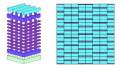
A comparison of mSATA (left) and M.2 (right) SSDs. Image courtesy of AnandTech
AAC: What role would you say firmware plays in how you designed this particular memory technology?
Doug: Firmware is definitely more important than ever before. But, luckily, the software building blocks that are built into operating systems (like Linux and Windows) know how to handle ideal block devices. And that's what the controllers that connect with NAND actually present to the outside world. So I'd say the trend is actually toward having a very efficient software stack.
So, for example, I'd say one of the standards that's becoming very strong in the SSD space is NVME, which is Non-Volatile Memory Express. It's a software protocol that standardizes putting non-volatile memory on the DCIE bus. That's not NAND-specific, of course, but NAND flash is really what NVME is about today.
Maybe in the future, there'll be non-volatile memories like MRAM (magnetoresistive random access memory) or ReRAM (resistive random-access memory) or something like that that are also non-volatile that'll be connected. But, for the foreseeable future, NVME drives (which are basically standardized DCIE-based SSDs) will be where it's happening. That's been an ongoing software development that really affects the storage architecture of the PC. And it's been a long time coming because it really tries to remove latency from the IO stack—within the software stack of the operating system. That wasn't standardized in the past because people just put non-volatile memory back closer to the processor. But NVME helps reduce latency and that's really the software architecture that will allow that to happen.
AAC: How has the fabrication process changed for you in this shift to 3D?
Scott: As we go from generation to generation in the 3D technology, the biggest notable change is that there's been approximately a 40% increase in the density per the die. That's significant. The desire in the industry is to have as much data as you can from the die in the package.
3D is about three to four times more expensive than floating gate. And a lot of that is because you need to have multiple etch and deposition machines that help with the layers of the 3D flash memory. Throughput on 3D is a lot different than the floating gate. We had our Fab 2 (fabrication facility in Yokkaichi, Japan), which was previously doing some back-end work. We took it back to the ground and re-built it to make it scale fast. That's dedicated 100% to the 3D production. Most recently, we announced that we started building Fab 6, which we're building in phases. The first half of Fab 6 is being built and the shell is expected to be done by summer of 2018.
We're watching the market so we get the right timing. We're bringing in the equipment to bring up that Fab to allow for the output that will help satisfy the demand in the market.

Image from the Toshiba Memory Blog
AAC: This new 3D memory still operates on silicon substrates, but we do see occasional materials come through that aim to unseat silicon. Can you comment on the material sciences of the memory industry?
Doug: For memory, silicon still seems to be the most economic choice. So we don't need the characteristics of III-V compounds like silicon carbide or gallium nitride. However, for other parts of the semiconductor industry, specifically things like power FETs, III-V compounds are very important for things like power switches. So I imagine that those two technologies will be used in any power electronic, whether it be lighting or electric cars or renewable energies or inverters. It'll possibly allow for smaller power converters in the future. But again, it's technology that's not required for memory devices at this point.
AAC: Do you think that pioneering a new material for memory could be something that you'll look to in the future?
Doug: Probably not at this point. A new material system will probably be necessary for things like ReRAM. To make ReRAM practical, we will have to have some other way of storing state information. Right now, all flash memory depends on electron storage of some sort. You're storing electrons to determine the state of that transistor to store data. But ReRAMs are fundamentally different. They're going to require some kind of slight material change at the atomic level. So certainly materials are going to be important for next-generation non-volatile memory, whether it be ReRAMs or MRAMs or something like that. Even in high-speed logic, you would have thought that the big processor manufacturers would have moved away from silicon. But that hasn't happened yet. There's not a good reason to have a non-silicon-based processor yet.
There isn't a good replacement yet for silicon. All the other alternatives are either more expensive or there's not a good reason to shift yet. A new material won't go into production unless it has a good economic reason to—or a good technical reason why something else doesn't work.
In the early days of electronics, people used Germanium but they found silicon to be far better. So that's why, in the 50s and 60s, everyone moved to silicon. They proved that silicon dioxide is so good that it's what really made FETs possible whereas the early transistors were mostly all bipolar transistors. Probably 99.999% of all transistors built today are FETs.

AAC: Did you feel that you were taking a risk in researching this 3D flash technology?
Scott: Obviously there's an advantage to flash technology and we're very purposeful in what we do. Looking towards the future, we knew that floating gate was reaching its end and that we had to research what other alternatives were there to continue leadership in the industry. With that, it came to utilizing the z-axis so, instead of doing the normal planar type of circuitry, we wondered what would happen if we took that and stacked it vertically. That's kind of the direction that everything went. But I don't know that there were much better alternatives out there. Floating gate just wasn't going to do it so I guess it's kind of natural.
AAC: So moving into the z-axis was the next logical step. What was the process of developing that like?
Scott: It's a fundamental shift in terms of memory development. It's very complex when you get down into it. Trying to bring 3D to market in the industry as a whole and to maturity has proven much more challenging than any of us thought it could be. We're just now getting more and more confident that we're going to be able to see the 3D technology in the market.
Doug: It has been a complex process. Certainly, building a shrink in planar was a lot easier! But, at some point, the number of electrons per cell got too small. You can only make the cell so small and, since we're still related to the same material system and we still need to store charge, there was a limit to how far we could actually shrink one memory cell in one plane.
So by going to 3D, we could make the memory cells bigger and we could store more charge and put the cells farther apart so they wouldn't interfere with each other (which is called inter-cell interference). And by just increasing the number of layers, we can increase the density of the die for the next generation. But it certainly has been a learning experience. Again, it's been more difficult than doing planar shrinks in the past but the industry as a whole is getting to 3D production pretty quickly. I think the estimate is that more than half the number of bits we create by the end of the year is going to be 3D. That's a pretty good transition if half the flash bits in the world are going to be 3D-based.

4th-gen Toshiba 3D flash memory is part of an increasing improvement from generation to generation.
AAC: What do you think accounts for how quickly this technology is being adopted and implemented?
Doug: I guess for the industry, itself, there's no choice! If flash memory was going to scale, there would have to be concerted effort to go into the 3D technology of some sort. Every NAND manufacturer had to go in that direction. There was no choice. The continued demand for flash and lower-cost flash and higher-density made this inevitable in some sense.
The Toshiba team is at the Flash Memory Summit this week in Santa Clara!
Related Content