Facebook
 Google
 GitHub
 Linkedin
UK Researchers Tweak Semiconductor Properties by Manipulating Adjacent Crystals
Researchers at the University of Manchester’s National Graphene Institute have shown how the properties of a material made from layers of atomically thin semiconductors can be precisely altered by rotating the position of adjacent crystals.
Since graphene was first isolated back in 2004, coincidentally at the University of Manchester, researchers have identified a vast range of 2D materials each with their own specific properties. By stacking these thin crystals together, many artificial heterostructure materials have been made.
Although several studies have demonstrated that these heterostructures can be refined by adjusting the rotation of adjacent crystals, these have been limited to graphene and hexagonal boron nitride.
Understanding TMDs’ Electronic Properties
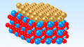
Now, a new study by researchers at the University of Manchester’s National Graphene Institute (NGI) has shown how the same technique can be used to tweak the properties of transition metal dichalcogenides (TMDs), a class of atomically thin semiconductor that holds a lot of promise for electronics applications.
The team’s research was published in the journal Nature Nanotechnology and describes how small rotations of a TMDs’ atomic lattices adjust locally to form perfectly stacked bilayer islands.
Using atomic resolution transmission electron microscopy (TEM), the University of Manchester researchers have demonstrated that stacking the two monolayers almost parallel to one another (with a twist angle close to 0°) and anti-parallel (with a twist angle close to 180°) produces “strikingly different” periodic domain patterns.

Nanopatterning electronic properties. Image Credit: University of Manchester
A ‘Ground Breaking’ Impact on 2D Materials
"A fundamental understanding of the evolution of crystal structure in twisted transition metal dichalcogenides is critical to the study of their exciting electronic and optical properties and was missing in the field,” says Astrid Weston, a research physicist working on the project.
The electronic properties of 2D materials are thought to depend on the local atomic stacking configuration, and such periodic domain networks could open up a way to pattern material properties with nanometer precision.
The Manchester team has found that the domain in almost-parallel bilayers demonstrates “intrinsic asymmetry of electronic wavefunctions previously unseen in other 2D materials.” According to them, this “twist” degree of freedom in heterostructure design could enable the development of new quantum systems such as single-photon emitters.