Facebook
 Google
 GitHub
 Linkedin
Xilinx Brings FPGA DNA to a Custom Hybrid System-on-Chip for 5G Radio Units
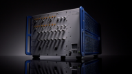
Xilinx solutions are surfacing for each new wave in the 5G rollout. Appearing in 2021, the new RFSoC DFE is forecasted to break all existing benchmarks.
The nature of 5G networks is based on a disaggregated design for fronthaul between the radio unit (RU) and the distributed units (DU), midhaul with the centralized units (CU), and the backhaul into the core networks.

The O-RAN 5G network topology, showing the disaggregated network split between different processing units and data hauls. Image used courtesy of Nokia
Since 2018, Xilinx has been hard at work engineering solutions for each stage in the 5G chain. Just last month, Xilinx introduced the T1 Telco accelerator card for fronthaul and midhaul operations.
Now to challenge the market, Xilinx is providing a new "breakthrough technology" across multiple business cases by innovating, optimizing, and hardening IP cores into the new Zynq RFSoC DFE (digital frontend).
The Need to Upgrade from 4G Hardware
We recently interviewed the team at Xilinx on this upcoming technology. According to Gilles Garcia, Senior Director of Marketing and WW Channel Business Lead at Xilinx, 5G business cases are fundamentally different from 4G.
4G technology was a closed ecosystem between OEMs, operators, and cellular users, Garcia explains. Comparatively, the 5G model incorporates not only wireless operators but also content providers, private networks, wireless OEMs, and many other new markets. ASICs were dominant in the 4G ecosystem, but there was a high-cost NRE associated with the ASIC model.

The theoretical differences between 4G and 5G. Image used courtesy of Thales Group
"For the first time, Xilinx is providing a wireless platform with more hardened IP than adaptive logic in an effort to address the specialized needs of 5G,” said Liam Madden, Executive VP and General Manager of the Wired and Wireless Group at Xilinx.
Madden goes on to explain that “with the market needs around 5G evolving, integrated RF solutions need to be adaptable to address future standards while also meeting demanding power, performance, and cost requirements.”
The Breakdown of the New SoC
The new Zynq RFSoc DFE is an adaptive radio platform composed of three major system elements:
- IP-hardened RF and digital frontend
- Optimized soft-logic FPGA fabric
- Multi-core Arm processing unit

The hybrid Zynq RFSoC DFE, a first for Xilinx combining their FPGA DNA with a new hardened digital front-end and an Arm processor. Image used courtesy of Xilinx
The chipset is designed to meet the current and future needs of the diverse 5G ecosystem with multiband support of the sub-6GHz and millimeter frequency bands, multi-carrier capabilities, and support for GaN power amplifiers (with digital pre-distortion).
How Does this SoC Compare to Previous Zynq RFSoC Generations?
Compared to the current Gen 3 Zynq RFSoC, the new chipset shines in three key benchmarks, according to Xilinx.
First, the new silicon offers two times the compute processing of the previous generation. The second benchmark revealed a 50% total power reduction over the Gen 3 chipset. This reduced power requirement was actualized through the hardened RF frontend along with the FPGA soft-logic.
Finally, the most nuanced breakthrough lies with the optimized soft-logic (FPGA), which can be interleaved with the hardened IP blocks. This alters how the digital frontend operates, even bypassing chain elements altogether in some instances. This is where the Zynq RFSoC DFE really outshines ASICs in terms of flexibility.

Block diagram of the RFSoC DFE. Units include digital up/down converters, equalization, a 32G SerDES, and ADC/DAC units. FPGA soft-logic interleaving allows for deep customization of the chip functionality. Image used courtesy of Xilinx
Engineers in charge of lifecycle management might take note of the chipset's pin compatibility with the current generation 3 Zynq RFSoC—that is, with proper engineering considerations and an identical package. This ensures that Gen 3 units can be upgraded with limited additional cost to the DFE, protecting operator investment as 5G evolves.
Why Radio Bandwidth Optimization and O-RAN are Critical to 5G
Spectrum demand and carrier aggregation of 4G/5G mixed-radio use is driving the demand for larger operating bandwidths from radio frontends. Xilinx claims that currently, the RFSoC DFE is the industry’s only 400 MHz instantaneous bandwidth-capable radio platform. It allows for 4G/5G to be run on the same radio unit.
As one of its core values, O-RAN encourages competition—providing an open topology for multiple entrants into the 5G market. As a cost-advantaged solution for lower-volume operators (when compared to an ASIC), Xilinx envisions many possible implementations of their technology in the RU.
Perhaps the most exciting business case possible with this hybrid chipset revolves around RAN sharing, where multiple operators share a single radio unit through time/frequency division multiplexing (TDD/FDD).

Multiple operators or mobile technologies (4G LTE & 5G) can share a single radio unit with eight transmit/eight receive split between them. Image used courtesy of Xilinx
The disparate nature of 5G aligns with the deep customization and acceleration technologies possible with FPGA fabric. Xilinx is all-in with O-RAN, providing solutions up and down the entire 5G data link.
The so-called next-gen SoC may provide operators with future-proofed assets capable of adapting to the changing standards, possible applications, and market demand for more bandwidth. The faster processing and lower power consumption mean a lower total system cost with fewer units and power stages doing the work of previous generations of radio technology.
Related Content