 Facebook
 Google
 GitHub
 Linkedin
A Simple, Compact Power Supply for Analog and Mixed-Signal Systems
This project demonstrates and discusses the performance and functionality of an inductorless ±5 V power-supply circuit.
This project demonstrates and discusses the performance and functionality of an inductorless ±5 V power-supply circuit.
Before you dive into building your own circuit, I highly recommend you take a moment to look at a few supporting articles (if you haven't already). These articles will help give a background and understanding of power supplies and their design.
- Boosting and Inverting without Inductors: Charge-Pump Power Supplies
- Designing a Charge-Pump Bipolar Power Supply
- PCB Layout for a Charge-Pump Bipolar Power Supply
I recently designed a power-supply circuit that takes a 5 V input and generates low-noise 5 V and –5 V outputs. It’s a straightforward circuit that doesn’t require much design effort or board space, and you can easily adjust the output voltages by changing two resistors. I think that it would be a great circuit for low-current analog and mixed-signal systems that need symmetric supplies, and with this project, I’ll try to give you the information you need to decide if it would be a good option for your particular application.
This article already has numerous images, so check out the previous articles if you'd like to see the project's schematic and the PCB layout.
The Board
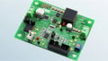
Here is a photo of the inductorless ±5 V power-supply subsystem:

I ordered the PCB from OSH Park and installed the surface-mount components using bismuth-based solder paste and a hot-air gun. I had to use an iron to fix one solder bridge and clean up a few joints, but overall the process went quite smoothly. The crooked parts are proof that I assembled it myself.
Load Regulation
The circuit is built around the LTC3265. This IC gives you four output voltages; two are the outputs directly from the charge pumps, and the other two are the charge-pump outputs regulated by an LDO. One of the first things we want to know is how well the outputs maintain their voltage under varying load conditions.
The following table reports the voltages produced by the LTC3265 with four different values of load resistance. The load resistors are connected to the LDO outputs, but as you will see, they affect the direct-from-the-charge-pump outputs as well. The maximum output current of the LDOs is 50 mA (i.e., you get 50 mA from the positive LDO and 50 mA from the negative LDO), so a resistance of 100 Ω corresponds to full load.
| +10 V supply | –10 V supply | +5 V supply | –5 V supply | |
| 10 kΩ | 9.84 V | –9.77 V | 5.00 V | –4.94 V |
| 1 kΩ | 9.57 V | –9.39 V | 5.00 V | –4.94 V |
| 470 Ω | 9.24 V | –8.94 V | 5.01 V | –4.94 V |
| 100 Ω | 7.01 V | –5.60 V | 5.02 V | –4.92 V |
The bottom line here is that the load regulation of the LDO outputs is very good, and that of the charge-pump outputs is terrible. However, this is by no means a criticism of the LTC3265, because I assume that the charge pumps are intended only to feed the LDOs, not to function as independent supplies. But it’s still important to be aware of this behavior because it means that you have to be very careful if you want to use this one IC to generate four supply rails instead of two. As far as I know, this could be done, but the two non-LDO outputs would be noisier than the LDO outputs, and their voltages would be much less predictable.
Also, I’m not sure why the amplitude of the negative output is slightly lower than that of the positive output. If this is an issue in your application you could compensate by adjusting the resistive divider that controls the LDO voltage.
Noise Performance
This reference design is intended as a bipolar power supply for analog and mixed-signal circuits and, consequently, noise is a major concern. Based on my measurements, I would say that the LTC3265 is a good choice for noise-sensitive applications. There is no doubt that the charge-pump outputs will be noisy, but the LDOs effectively suppress the ripple.
The following eight images were captured from my MDO3104 oscilloscope from Tektronix; they show you the noise in the ±10 V outputs and the ±5 V outputs for four different values of load resistance (yellow is always the positive voltage, and blue is always the negative voltage). The ±10 V captures are followed by the ±5 V captures, so you can see the noise reduction provided by the LTC3265’s linear regulators. Again, the load resistors are always connected to the LDO outputs. Also, note that for convenience I’m referring to the direct-from-the-charge-pump voltages as the ±10 V outputs, despite the fact that the voltage drops significantly at higher load currents.

±10 V, 10 kΩ

±5 V, 10 kΩ

±10 V, 1 kΩ

±5 V, 1 kΩ

±10 V, 470 Ω

±5 V, 470 Ω

±10 V, 100 Ω

±5 V, 100 Ω
All of the captures have the same vertical and horizontal scale, so you can make direct comparisons. The noise-reducing action of the LDO is most apparent in the 100 Ω plots; it does a great job of removing the low-frequency ripple. The high-frequency spikes are more troublesome.
The spikes are clearly periodic, with a frequency of about 1 MHz, which isn’t too surprising considering that the LTC3265 was switching at 500 kHz. The noise level between the spikes (about 35 mV peak to peak) is quite good. The amplitude of the spikes is significant, but in my opinion, the spikes are not very concerning because high-frequency energy such as this is easily filtered out in low-current applications. If I were to redesign this board I would definitely use a ferrite bead to form a low-pass filter on the LDO outputs. (This approach is less feasible in high-current circuits because more voltage will be dropped across the DC resistance of the bead.)
The next two captures give you a close-up view of the spikes.

Close-up view of noise spike, ±10 V, 470 Ω

Close-up view of noise spike, ±5 V, 470 Ω
Burst Mode
All the previous measurements were gathered with the LTC3265 in constant-frequency mode. This is probably the preferred mode in most applications because it gives you lower noise. The alternative is burst mode, which reduces power consumption and thus could be better for battery-powered devices. The next set of scope captures gives you an idea of burst-mode noise performance.

±10 V, 470 Ω, burst mode

±5 V, 470 Ω, burst mode

±5 V, 470 Ω, burst mode, close-up view of noise spike

±5 V, 100 Ω, burst mode
Once again, we see that the LDO is very effective when it comes to suppressing lower-frequency noise. Note also the temporal irregularity of the noise in the ±5 V outputs (particularly the negative voltage) with 470 Ω load resistance.
Switching Frequency
One thing I’m not sure about when it comes to the LTC3265 is the switching frequency. The datasheet indicates that you can control the switching frequency by varying the amount of resistance between the RT pin and ground. My board has a potentiometer that allows me to easily adjust the RT resistance, but I didn’t see any change in the frequency characteristics of the output voltage.
I used my DMM to confirm that the potentiometer was functional and was, in fact, varying the resistance between RT and ground. The only thing I’m not sure about is whether this change in resistance actually controls the periodic characteristics of the output ripple. The datasheet’s section entitled “Charge Pump Frequency Programming” discusses the effect of switching frequency on charge-pump output resistance and on burst-mode performance, but it doesn’t say anything about output ripple.
Conclusion
I hope I’ve provided enough data to help you determine whether this power-supply circuit, or something similar, would be a beneficial addition to your next analog or mixed-signal project. I’ve included a short video showing the difference between the ±10 V outputs (the first pair of waveforms) and the ±5 V outputs (the second pair of waveforms) with a load resistance of 470 Ω, in burst mode. After the video, you’ll find a link that you can use to download the DipTrace schematic and layout files.
Inductorless_Bipolar_Power_Supply.zip
Related Content


A very helpful article and a handy chip too. The problem with not being able to modify the switching frequency may be down to the potentiometer value used - the PCB layout indicates that a 1KOhm pot was used, but the LT3265 datasheet indicates that a 1MOhm span would be needed to modify the frequency from 500KHz down to below 100KHz (and the frequency stays at 500KHz from 1KOhm up to around 11KOhm, by the look of it)...
I have no problem except the statement that the charge pump output would probably be more stable if it went through the LDO. I don’t think it is possible to use an LDO regulator to output 10 V when the charge pump can’t output less than 10 V, which is the case in this demo. Can the chip be adjusted to output >10V?