Facebook
 Google
 GitHub
 Linkedin
An Arduino-Compatible Relay Controller for RS-485 Networks
This project brief describes how to build and use an Arduino-compatible relay interface board that switches a 10 A load over an RS-485 network.
The RS-485 Relay Interface Board is an Arduino-compatible module built around an ATmega328 microcontroller and a Texas Instruments SN65HVD08DR half-duplex RS-485 transceiver. The board pairs that communication link with a 5 V relay driven through a BC847 BJT, so a command sent over an RS-485 bus can switch a load rated up to 10 A. The assembled board is shown in Figure 1.
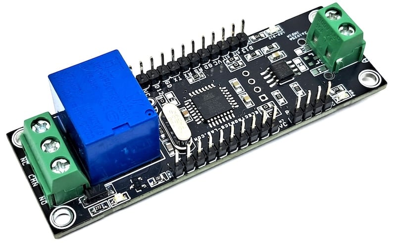
Figure 1. The assembled RS-485 Relay Interface Board.
Screw terminals bring out the RS-485 A and B lines and the relay's common, normally open, and normally closed contacts, while header connectors expose the remaining I/O for expansion.
A simple ON/OFF application demonstrates the design: a host node on the RS-485 bus sends a command, and the board's relay switches in response.
The board also carries headers for an optional 0.96-inch OLED display and an optional 433 MHz ASK RF module, plus onboard LEDs for power, relay state, and a general-purpose function LED tied to D13.
Specs and Features
- Supply voltage: 5 V DC
- Relay contacts: 5 V relay rated 10 A (normally open and normally closed)
- RS-485 communication, half-duplex, via SN65HVD08DR transceiver
- Screw terminal for RS-485 A/B connection
- RS-485 bus-open, short-circuit, and idle-bus failsafe receiver
- Multiple I/O lines available through header connectors
- Onboard power LED, function LED (D13), and relay LED
- Optional 0.96-inch OLED display, mounted on the underside of the board
- Optional 433 MHz ASK RF module header
- Four 3 mm mounting holes
- PCB dimensions: 79.22 x 26.51 mm
How It Works
An ATmega328 microcontroller manages the board's I/O and drives the RS-485 link. Its pins connect to the SN65HVD08DR transceiver as follows: RO to D10, RE to D2, DE to D3, and DI to D11. RE and DE together form the transceiver's direction control, letting the microcontroller switch the half-duplex bus between transmit and receive.
The SN65HVD08DR runs from a 3 V to 5.5 V supply, draws less than 90 mW of quiescent power, and is electrically compatible with the ANSI TIA/EIA-485 standard. Its open-circuit, short-circuit, and idle-bus failsafe receiver keeps the output in a known state even when the bus is unpowered or unterminated, and its 1/8-unit load rating allows up to 256 nodes on a single bus.
The relay is driven from D5 through a BC847 BJT, with a 1N4007 diode across the relay coil to clamp the flyback voltage when the coil switches off. A dedicated LED (D3) indicates relay state, alongside a power LED (D2) and a function LED (D1) wired to D13 for general status or debug use.
The board is programmed through a dedicated 8-pin bootloader and programming connector, CN4, which brings out TX, RX, reset, ground, VCC, and the D11/D12/D13 SPI lines. An external Arduino Uno can serve as the programmer: wire its TX, RX, VCC, GND, reset, and D11–D13 pins to CN4 as shown in Figure 2, then bootload and upload firmware through the Arduino IDE.
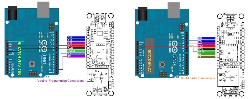
Figure 2. Arduino programming and bootloader connections at CN4.
For applications that need a local display, the board provides a footprint for a 0.96-inch I2C OLED display on its underside, wired to CN3 (VCC, GND, SCL, SDA).
Schematic and Bill of Materials
The full schematic is shown in Figure 3.
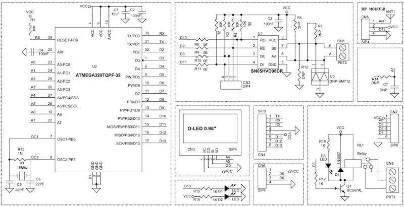
Figure 3. Schematic of the RS-485 Relay Interface Board.
The bill of materials is shown in Table 1.
Table 1. BOM for the RS-485 Relay Interface Board.
| REF | DESCRIPTION | QTY | MFG | SUPPLIER | PART NO. |
| CN1 | 2-pin screw terminal, 5.08 mm pitch | 1 | Phoenix | DigiKey | 277-1247-ND |
| CN2, CN3, CN5, CN6 | 4-pin male header, 2.54 mm pitch | 4 | Wurth | DigiKey | 732-5317-ND |
| CN4 | 8-pin male header, 2.54 mm pitch | 1 | Wurth | DigiKey | 732-5321-ND |
| CN7 | 6-pin male header, 2.54 mm pitch | 1 | Wurth | DigiKey | 732-5319-ND |
| CN8 | 3-pin screw terminal, 5.08 mm pitch | 1 | Phoenix | DigiKey | 277-1248-ND |
| C1 | 10 uF / 16 V ceramic, 0805 | 1 | Yageo/Murata | DigiKey |
|
| C2, C3, C4 | 100 nF / 50 V ceramic, 0805 | 3 | Yageo/Murata | DigiKey |
|
| C5, C6 | 22 pF / 50 V ceramic, 0805 | 2 | Yageo/Murata | DigiKey |
|
| D1, D2, D3 | LED, red, 0805 | 3 | OSRAM | DigiKey | 475-1278-1-ND |
| D4 | 1N4007 | 1 | Diodes Inc. | DigiKey | S1MBDITR-ND |
| Q1 | BC847AL | 1 | Nexperia | DigiKey | 1727-2924-2-ND |
| RL1 | 5 V relay | 1 | American Zettler | DigiKey | 3385-AZ943-1CH-5DE-ND |
| R1, R2, R3, R4, R5 | 10 kΩ, 5%, 0805 | 5 | Yageo/Murata | DigiKey |
|
| R8, R9, R10, R11 | 0 Ω, 5%, 0805 | 4 | Yageo/Murata | DigiKey |
|
| R13 | 1 MΩ, 5%, 0805 | 1 | Yageo/Murata | DigiKey |
|
| R15, R16, R17, R18 | 1 kΩ, 5%, 0805 | 4 | Yageo/Murata | DigiKey |
|
| U1 | SN65HVD08DR, SOIC-8 | 1 | TI | DigiKey | 296-39173-1-ND |
| U2 | ATmega328, TQFP-32 | 1 | Microchip | DigiKey | ATMEGA328-AU-ND |
| X1 | 16 MHz crystal | 1 | ECS Inc. | DigiKey | X1103-ND |
Connections
The board's connectors and header pinouts are shown in Figure 4.
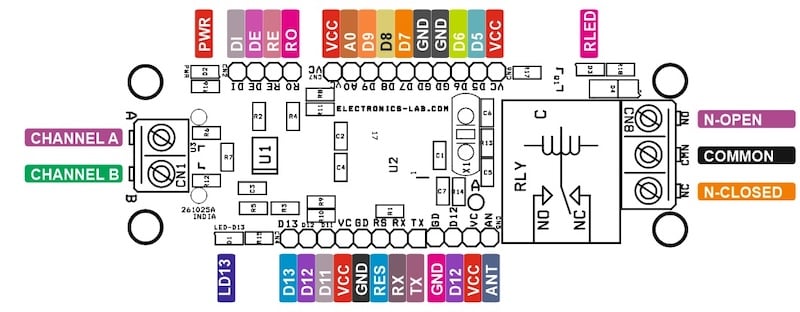
Figure 4. Connector and header pinout of the RS-485 Relay Interface Board.
CN1 — RS-485 Bus (2-pin screw terminal):
- Pin 1 = RS-485 Channel B
- Pin 2 = RS-485 Channel A
CN2 — Optional (not used):
- Reserved, no connection required
CN3 — OLED Display (4-pin header):
- Pin 1 = VCC
- Pin 2 = GND
- Pin 3 = SCL
- Pin 4 = SDA
CN4 — Programming/Bootloader (8-pin header):
- Pin 1 = TX
- Pin 2 = RX
- Pin 3 = Reset
- Pin 4 = GND
- Pin 5 = VCC
- Pin 6 = D11
- Pin 7 = D12
- Pin 8 = D13
CN5 — 433 MHz RF Module (optional, 4-pin header):
- Reserved for optional ASK RF module and antenna
CN6 — General I/O (4-pin header):
- Pin 1 = VCC
- Pin 2 = D5
- Pin 3 = D6
- Pin 4 = GND
CN7 — General I/O (6-pin header):
- Pin 1 = VCC
- Pin 2 = A0
- Pin 3 = D9
- Pin 4 = D8
- Pin 5 = D7
- Pin 6 = GND
CN8 — Relay Contacts (3-pin screw terminal):
- Pin 1 = Normally Closed
- Pin 2 = Common
- Pin 3 = Normally Open
U4 — Auxiliary Header (3-pin):
- Pin 1 = VCC
- Pin 2 = Analog A1
- Pin 3 = GND
PCB Files
The PCB layout, top and bottom copper layers, and board dimensions are shown in Figure 5.

Figure 5. PCB layout of the RS-485 Relay Interface Board.
You can download the layout files for this project here:
RS-485 Relay Interface Gerber Files
Except where noted, all images used courtesy of Rajkumar Sharma