 Facebook
 Google
 GitHub
 Linkedin
Build a Development Platform for a PICAXE 40X2
The PICAXE 40X2 features 32 I/O ports and speeds up to 64MHz; a development platform simplifies project design using this workhorse.
The PICAXE 40X2 features 32 I/O ports and speeds up to 64MHz; a development board simplifies project design using this workhorse.
Project Overview
This article describes the PICAXE 40X2 microcontroller and defines the construction of a PCBA (printed circuit board assembly) that provides easy access to the µC's power connections, programming pins, and I/Os (inputs/outputs). If you are new to PICAXE microcontrollers, you would benefit from reading the introductory articles already published on All About Circuits, many of which are listed here.
The photo below shows two versions of the PCBA. At the top is a fully-featured version that includes a power regulator section and the necessary complement of header pins to easily and quickly connect the 40X2 to a solderless breadboard. It also includes a ceramic resonator that allows operation of the microcontroller at speeds up to 64 MHz. At the bottom of the photo is the minimalist version, which is well-suited for being built into robots, weather stations, musical instruments, or any other project that requires a microcontroller with up to 32 I/O ports.

Are More I/Os Better? Meet the PICAXE 40X2!
Some microcontroller experimenters (including yours truly) like to use small devices with a low number of I/Os, and squeeze as much as possible from them. Here's an example of a PICAXE project that accomplishes quite a lot with a PICAXE 08M2 and only five I/Os.
However, there is something to be said for using a big honking µC with enough connection points to let your imagination run wild. In the PICAXE family, the top dog is the 40X2 with 32 I/O ports. The 40X2 is based on the Microchip 18F45K22, and in fact, still bears that model number even after being converted to run PICAXE basic.

The PICAXE 40X2 is available in both a through-hole .6" DIP-40 and a surface-mount TQFP-44 package. (DIP is an abbreviation for Dual In-line Pin or Dual In-line Pack, and TQFP is an abbreviation for Thin Quad Flat Pack.) The pinouts for both packages are shown in the figure below.

If you are familiar with the PICAXE family, you may recall that in PICAXE parlance, the metal pieces protruding from the perimeter of the chips are called "legs," and the term "pin" is used in the designation for each of the I/Os. For example, in the TQFP-44 drawing above, leg 1 at the upper left corner is the electrical connection point for pin C.7. This is important to remember because the schematic diagram references leg numbers while the code references pin designations. The practice is actually quite logical once you use it for a while.
At first glance, the DIP-40 and the TQFP-44 packages seem to have completely different capabilities, but a closer inspection dispels this notion. There are four extra legs on the TQFP-44 which are not used and are marked as "NC" in the pinout diagram; they are legs 12, 13, 33, and 34. Both packages offer exactly the same complement of I/O functions even though the leg numbers differ from one package to the other. See the table below, and consult PICAXE Manual 1 for more information on I/Os and how to use them.
| Pin | Function(s) Available | Pin | Function(s) Available |
|---|---|---|---|
| A.0 | In, Out, ADC0, Comp1-, touch | C.0 | In, Out, timer clk |
| A.1 | In, Out, ADC1, Comp2-, touch | C.1 | In, Out, pwm |
| A.2 | In, Out, ADC2, Comp2+, touch, DAC | C.2 | In, Out, pwm, hpwm A, ADC14, touch |
| A.3 | In, Out, ADC3, Comp1+, touch | C.3 | In, Out, hspi sck, hi2c scl, ADC4, touch |
| A.4 | Serial Out, Out, SRNQ | C.4 | In, Out, hi2c sda, hspi sdi, ADC16, touch |
| A.5 | In, Out, ADC5, touch | C.5 | In, Out, hspi sdo, ADC17, touch |
| A.6 | In, Out, ADC6, touch | C.6 | In, Out, hserout, ADC18, touch |
| A.7 | In, Out, ADC7, touch | C.7 | In, Out, hserin, ADC19, touch |
| B.0 | In, Out, ADC12, hint0, touch, SRI | D.0 | In, Out, ADC20, touch |
| B.1 | In, Out, ADC10, hint1, touch | D.1 | In, Out, ADC21, touch |
| B.2 | In, Out, ADC8, hint2, touch | D.2 | In, Out, ADC22, touch |
| B.3 | In, Out, ADC9, touch | D.3 | In, Out, ADC23, touch |
| B.4 | In, Out, ADC11, touch | D.4 | In, Out, ADC24, touch |
| B.5 | In, Out, ADC13, touch | D.5 | In, Out, hpwm B, ADC25, touch |
| B.6 | In, Out | D.6 | In, Out, hpwm C, kb clk, ADC26, touch |
| B.7 | In, Out | D.7 | In, Out, hpwm D, kb data, ADC27, touch |
As you can see, in addition to a large number of I/Os, the 40X2 has extensive functional capabilities. Add to that a top speed of 64MHz, and you have a very capable microcontroller. For a more complete description of the 40X2 features, have a look at this document.
Accessing 32 I/Os Presents Some Challenges
In the DIP-40 package, the 40X2 is over 2" long and .6" wide; it takes up a fair amount of real estate, especially on a solderless breadboard.

At just over 11mm by 11mm, the TQFP-44 package is smaller than a postage stamp, but those legs on .8mm centers don't lend themselves to easy connections. Of course, a breakout board is always possible, but then you are back to the DIP-40 size.

The obvious answer is to create a development/experimentation platform, and that is the approach that this article will explain. Read on!
The PA-40X2 BBA

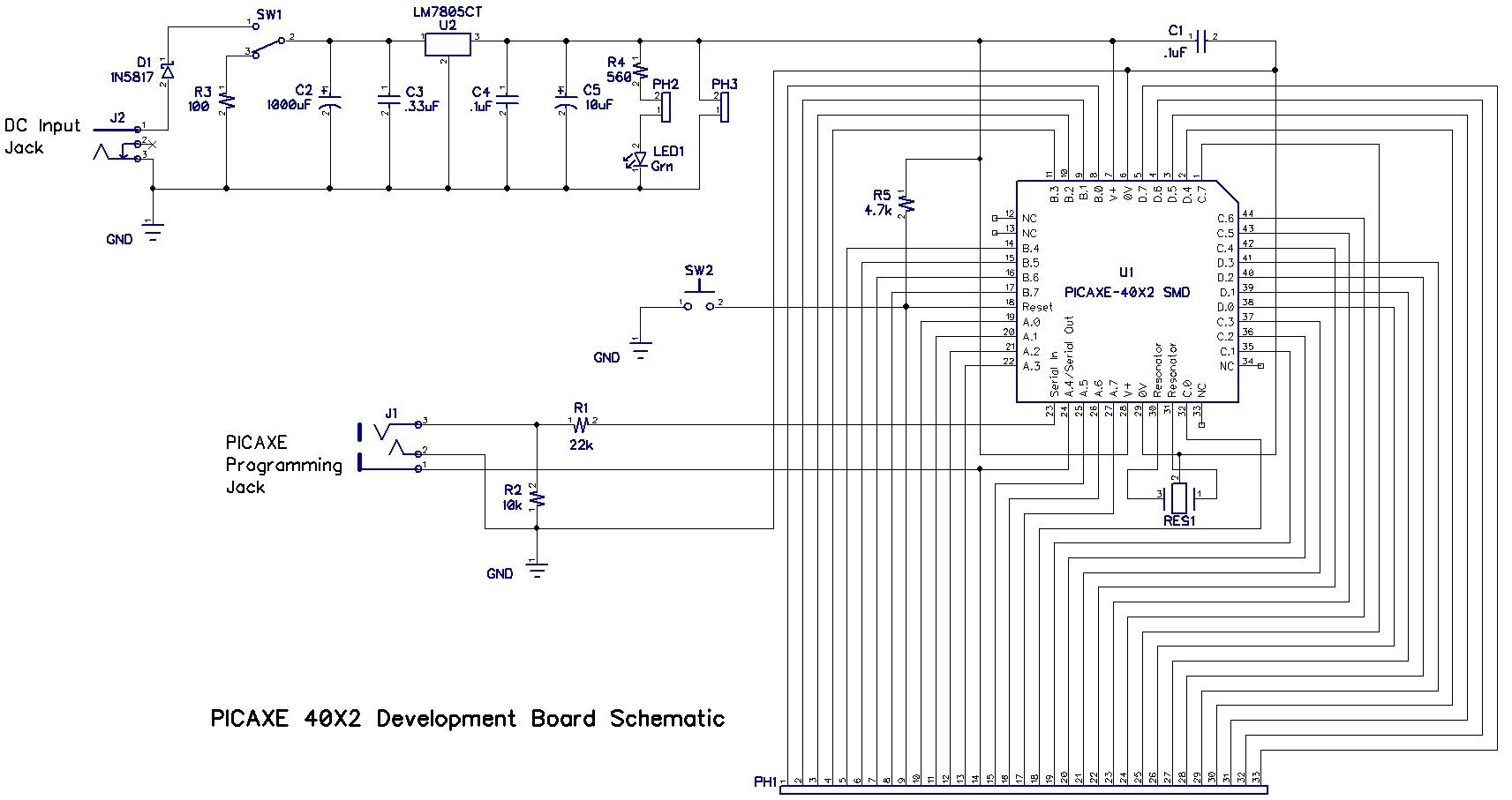
The photograph above shows the PA-40X2 BBA carrying a PICAXE 40X2 in the TQFP-44 package. The BBA assembly is connected to an 800-pin solderless breadboard via header pins that protrude from the bottom of the PCB into the solderless breadboard. Each of the 40X2 I/O's is brought out to the front edge of the PCB and connected to a header pin that extends out the bottom of the PCB, and inserts into a hole on the solderless breadboard. Each header pin is labeled on the PCB with the corresponding PICAXE I/O pin designation. There are two additional header pins that plug into the top power rail on the solderless breadboard and supply operating power. This arrangement provides an excellent development platform for the PICAXE 40X2.
Notice that the PCB includes the standard PICAXE programming circuit on the left side and a linear DC regulator along the back edge. A coaxial power input jack is located on the right edge and an on/off switch is at the top right.
A power-on LED indicator is at the top left; the shorting block can be removed when the LED is not needed or when power conservation is desired. The PCBA is complete with a reset pushbutton and a ceramic resonator for the PICAXE µC.
The photo below of the bottom side of the PCBA shows how the header pins that plug into the solderless breadboard are arranged. The two 1/2" standoffs that support the back edge of the PCB are also shown.

A schematic diagram of the circuit is shown immediately below, and is followed by a straight top-down view of the assembled adapter.

Parts List
| Reference No. | Description | Qty. | Source | Part Number |
|---|---|---|---|---|
| J1 | Jack, 3.5mm, 3 Conductor | 1 | Digi-Key | SC1458-ND |
| J2 | Jack, Power, Coaxial, 2.1mm Center Pin | 1 | Jameco | 2144690 |
| D1 | Diode, Schottky, 40V, 1A | 1 | Digi-Key | 1N5819-TP |
| R1 | Resistor, 22kOhm, .25W, Carbon Film, Axial Leads | 1 | Digi-Key | 22KQBK-ND |
| R2 | Resistor, 10kOhm, .25W, Carbon Film, Axial Leads | 1 | Digi-Key | 10KQBK-ND |
| R3 | Resistor, 100 Ohm, .25W, Carbon Film, Axial Leads | 1 | Digi-Key | 100QBK-ND |
| R4 | Resistor, 560 Ohm, .25W, Carbon Film, Axial Leads | 1 | Digi-Key | 560QBK-ND |
| C1, C3 | Capacitor, Ceramic, .33uF, 50V, Radial Leads | 2 | Digi-Key | 490-8842-ND |
| C2 | Capacitor, Electrolytic, 1000uF, 50V, Radial Leads | 1 | Digi-Key | UVY1H102MHD-ND |
| C4 | Capacitor, Ceramic, .1uF, 50V, Radial Leads | 1 | Digi-Key | 399-9877-1-ND |
| C5 | Capacitor, Electrolytic, 10uF, 50V, Radial Leads | 1 | Digi-Key | 493-5915-1-ND |
| RES1 | Resonator, 16.0000MHz, 15pF | 1 | Digi-Key | 490-7035-ND |
| PH1-PH3 | Header, Pin, Straight (Make from strip.) | 1 | Jameco | 2168211 |
| U1 | Microcontroller, PICAXE, 40X2, TQFP-44 | 1 | PICAXE.com | TQFP-44 40X2 |
| U2 | Regulator, Linear, 5V, TO-220 | 1 | Digi-Key | LM7805CT-ND |
| SW1 | Switch, SPDT, Slide, 500mA | 1 | Jameco | 109171 |
| SW2 | Switch, SPST, Pushbutton, Momentary, NO | 1 | Digi-Key | 450-1650-ND |
| N/A | Shunt, 2-Position, .1" Centers, Closed, Green | 1 | on-line search | N/A |
| N/A | Heat Sink, TO-220 | 1 | Jameco | 158051 |
| N/A | Grease, Thermal, Silicone, White | 1 | Jameco | 615312 |
| N/A | Spacer, Nylon, Tapped 4-40, .5" | 2 | Digi-Key | 36-1902C-ND |
| N/A | Screw, Machine, 4-40, Pan Head, Phillips, .25" | 3 | Jameco | 2094389 |
| N/A | Nut, Machine, 4-40 | 1 | Jameco | 40943 |
| N/A | Printed Circuit Board, Custom Made, FR4, 1.6mm Thick, 1 oz. CU | 1 | Itead | See the text. |
The PCB
The use of the surface-mount TQFP-44 40X2 made some vias necessary on the PCB layout and, for that reason, a home-etched board is probably not within the capabilities of many DIYers. So the best choice is one of a number of reasonably priced supply houses. Itead, a Chinese supplier, is dependable and produces a quality 2-sided board that's fairly priced at about $15 for 10 copies. Shipping can be as low as another $4-$5 if you're willing to wait three or four weeks. If not, there's an air express option for about $10 more.
Standard Gerber files are ready for download below, and should be perfectly acceptable for most board fabricators. The files are for non-commercial use and don't have a guarantee, but they were used to build the boards pictured in this article, and should work for you. DipTrace was used to draw the schematic diagram and lay out the PCB.
Assembly and Testing
All components on the PICAXE 40X2 BBA are through-hole with the exception of the 40X2 microcontroller. It's generally easier to install and solder the shorter components first; therefore, it is recommended that you start with the 40X2, and ensure that it is correctly installed with all solder bridges removed before installing the through-hole components. Be sure to note that with the 40X2 correctly oriented on the PCB, the text on the chip is upside down. The remaining assembly is straightforward; just follow the reference designations on the PCB, the schematic diagram, the photographs, and the parts list.
Once you have completed the assembly and double checked your work, apply from 7 to 15VDC to J2, and confirm that the green LED lights. Connect your PICAXE programming cable (AXE-027 or serial cable) to J1 and, using PICAXE EDITOR 6 (PE6) or the PICAXE IDE of your choice, confirm that you are able to communicate with and program the 40X2 µC.
Options
Although the 40X2 BBA is primarily intended for use with an 800-pin solderless breadboard, there are options.
- If your breadboard does not have a power rail identical to the one shown in the photographs, do not install the two header pins on the bottom of the PCB. Instead, you might install them on top of the PCB, and use a pair of female to male jumpers to connect to your solderless breadboard.
- If you do not wish to use a solderless breadboard at all, do not install any of the header pins on the bottom of the PCB. Instead, you might install them on top of the PCB, and use female to male jumpers to connect to your external assemblies.
- You don't have to install header pins at all. For example, you might solder wires directly to the pads on the PCB and use them to connect to your external assemblies.
- If you plan on running your project from an external power supply or from batteries, you can leave off the entire regulator section as shown in the photograph at the beginning of this article. Be careful to avoid reversing the polarity of the power connections and be sure not to exceed 5V as a power source; either mistake could permanently damage the PICAXE 40X2.
Use your imagination to find creative ways to use the 40X2 BBA in your next PICAXE project. Happy experimenting!
Give this project a try for yourself! Get the BOM.
Related Content


Excellent article, will be trying this out shortly!