Facebook
 Google
 GitHub
 Linkedin
Incorporating Wireless Power with IDT’s Tx/Rx Reference Kits
Two evaluation boards from IDT help you to quickly and conveniently integrate wireless power into your designs.
Two evaluation boards from IDT help you to quickly and conveniently integrate wireless power into your designs.
The Quest for Wireless Continues
Despite the ongoing proliferation of wireless technology in its various forms, we need only look up at the power lines to remind ourselves that metal wires are still the preferred way to transfer electrical power from source to load. But even this paradigm is subject to innovation, and one of the companies seeking to drive this innovation is Integrated Device Technology (IDT). In this article we will explore a wireless power solution comprising evaluation boards for IDT’s P9038 transmitter IC and P9025AC receiver IC.
But First: Why Wireless Power?
Before you make haste to incorporate wireless power transmission into your latest gadget, take a good look at the bill of materials that will be used to replace a few copper wires:

Two sophisticated ICs, numerous passive components, an enormous transmitter coil, a somewhat less enormous charging coil, two carefully designed PCBs. . . . It is only fair to make the initial assumption that cables and connectors are here to stay. But the issue is not that simple, so let’s briefly discuss some benefits of wireless power.
First, it must be acknowledged that wireless power transmission appeals to the innate human appreciation for the new and different. This is not the sort of cost vs. benefit analysis you will see in an engineering textbook, but it is reality, especially in the context of the consumer electronics market. There are, however, advantages of a more “scientific” nature, most of which are related to the absence of connectors. A $500 battery-powered gadget is worthless if you can’t recharge it because a connector has failed in some way or another—contacts corrode, housings get dented, pins get bent, contact plating wears off, spring contacts become less springy. Connectors also are an impediment to a truly waterproof product; with wireless power transmission, fully submersible portable devices become much more feasible. And then there is the compatibility issue: fewer connectors means fewer problems with maintaining mechanical harmony between old and new hardware or between products from different manufacturers.
We also need to keep in mind that the device itself needs only the receiver portion of the wireless power transmission circuitry. The bulkier (and more expensive) portion is the transmitter, but ideally the transmitter would be incorporated into a standardized wireless charging module. Thus, a person might own half a dozen wirelessly powered gadgets but only one charging station that is compatible with all the gadgets. It is true that the receiver—at about 3 cm × 6.5 cm—is not exactly “compact” by today’s standards, but there are certainly many products that could find a place for this module simply because it is so thin.

The Evaluation Board Pair
The P9038 and P9025AC evaluation boards together form a 5 Watt, Qi-compliant wireless power solution. The Qi (pronounced “chee”) standard is an established set of guidelines for designing devices that incorporate inductive or resonant power transfer. Inductive power transfer requires that the transmitter and receiver be fairly well aligned and separated by less than approximately 7 mm; resonant power transfer is more flexible in terms of alignment and separation distance, but at the cost of lower efficiency and in some cases higher levels of electromagnetic interference (EMI). The boards discussed in this article utilize inductive power transfer.
IDT emphasizes that these reference kits are not what we usually think of as evaluation boards. They are primarily intended not for experimentation but rather for rapid integration into existing or forthcoming designs. The board layouts are optimized in terms of performance and size, with minimal provision of test points, headers, or other components that would facilitate extensive evaluation. Along with the boards themselves, IDT supplies schematics, gerber files, layout guidelines, and various other digital resources. Here is the rather extensive list of technical documentation for the receiver board:

To Evaluate: Plug In, Stack Boards
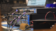
It doesn’t take much effort to get 5 Watts of wireless power out of these boards. Connect the transmitter board to a USB charger via the Micro-B connector, place the receiver board on top (as shown in the following image), and wait for the green LED on the receiver to indicate that you have 5 V at the output terminals.

A blinking green LED on the transmitter board indicates successful power transfer, and a solid red LED means that power transfer has ceased, presumably because of excessive distance or misalignment between transmitter and receiver.
Let’s solder some wires to the GND and OUT terminals so we can take a closer look at the power supply characteristics of the Tx/Rx pair. The receiver module is essentially a full-bridge synchronous rectifier that powers a low-dropout voltage regulator. The nominal output voltage is 5.3 V, as confirmed by the scope, and the rated output current is 1 A (absolute maximum 1.5 A).

We can collect a few data points to assess the load regulation capabilities of the output stage. (All the measurements in this section assume optimal alignment between transmitter and receiver.) At no load, the output is 5.34 V, as shown above. The following table gives the output voltage as load current increases.
| Load | Output Voltage | Output Current |
| 50 Ω | 5.28 V | 106 mA |
| 33 Ω | 5.24 V | 159 mA |
| 25 Ω | 5.22 V | 209 mA |
| 13 Ω | 5.20 V | 400 mA |
Thus, over this range of moderate output current, we have a 1.5% reduction in output voltage. This is somewhat higher than what we would expect from a standard linear regulator IC, but it is certainly not a serious concern, especially considering that most applications will regulate the P9025AC’s output down to a lower voltage.
Measurements taken with an additional 3 mm of separation between transmitter and receiver indicate that load regulation is not negatively affected by moderate increases in separation distance.
Now let’s take a look at the output noise. This first scope trace is the output noise at no load.

Here we see 15 mV peak-to-peak output ripple, which is quite good—in fact, 15 mV peak-to-peak is a respectable noise spec for standard switching regulators, which receive input power through a copper PCB trace rather than an oscillating magnetic field. The frequency of the noise, however, could present problems for highly sensitive applications. At 120 kHz, this ripple would be more difficult to filter out than noise from switching regulators, many of which now operate at frequencies above 1 MHz.
Here is the output noise with 400 mA load current:

The frequency is higher, but the important point is that the amplitude is about the same. This indicates that the output noise does not vary significantly with load current, which is a good thing. The following trace is the noise with 400 mA load current and an additional 3 mm of separation between the transmitter and receiver.

Based on these results, it appears that the P9025AC’s output noise is not greatly affected by moderate variations in load current or separation distance.
Proximity and Alignment
The measurements presented above give us reason to believe that these IDT reference kits can achieve a stable, low-noise wireless power supply—if, that is, the boards are properly aligned and separated by an appropriate distance. In other words, if you want reliable performance, your device must impose mechanical constraints that ensure an acceptable spatial relationship between transmitter and receiver.
First let’s consider the operational limits. The output voltage will be automatically deactivated under the following conditions:
- when the distance between the transmitter coil and the receiver coil exceeds approximately 18 mm
- when the misalignment exceeds what is depicted in the following three images


The next question is, what happens in between the optimal separation/alignment and the limits at which the output is definitively deactivated? The answer to this question is best conveyed by the following videos.
As you can see, the transition between operational and nonoperational is not a particularly smooth one. Output voltage gradually decreases as separation distance or degree of misalignment increases, and in the case of misalignment, the output voltage experiences some painful fluctuations before it is finally silenced. The transitional voltages displayed in these videos could lead to some seriously unpredictable circuit behavior, and thus we need to emphasize what was said at the beginning of this section: wireless power transfer, especially inductive power transfer, requires careful attention to alignment and separation between transmitter and receiver.
Recap
The P9038 and P9025AC evaluation kits from IDT are an excellent springboard into the steadily expanding world of wireless power. They allow for rapid prototyping and near-seamless integration into many devices, and the abundance of technical information and design support resources should greatly facilitate any modifications or customizations that you need to make. The quality of the output voltage seems more than adequate for digital and mixed-signal applications, especially given the ease of further regulating a 5.3 V supply down to the lower voltages commonly required by digital and analog ICs. The most prominent failure mode is related to improper spacing and alignment, so mechanical constraints must be included as an integral part of the design effort. The next article in this series will analyze the degree to which EMI generated by the power transmitter board degrades the performance of mixed-signal circuitry.
Give this project a try for yourself! Get the BOM.