 Facebook
 Google
 GitHub
 Linkedin
Tamper Detection with Differential Inductive Sensing Coils
This article demonstrates the creation of an inductive switch cabinet lock that can detect the movement of a conductive target. The purpose is to create a door that cannot be opened without triggering an alarm.
The LDC0851 is an inductive sensor IC that can detect changes in relative inductance. This article uses it to create an ultra-low-power circuit that can operate for months or years on a single button-cell battery to indicate when a cabinet door is opened.
About this Project
This project makes use of a free WEBENCH design tool from Texas Instruments to create an alarm circuit for a standard cabinet lock using a differential inductive-sensing alarm circuit. This project demonstrates PCB-based inductive sensor creation, as well as an application of the LDC0851 (PDF) from TI.
The circuit has no moving parts that can fail and uses a timer to achieve ultra-low power consumption, allowing a single button cell battery to power the circuit for years. The design is built around a standard cabinet-grade cam lock and creates a lock that can be picked or otherwise defeated but cannot be opened without triggering an electronic circuit. This is purely a demonstration project; the circuit could be used for pharmaceutical access control (e.g., PCA Infusion Pumps), desk and cabinet lock monitoring, stock control, utility meter tamper detection, and so forth.


Figure 1. First Circuitboard Designed in Altium's Circuitmaker (Left) and the Next Design Iteration Created in Diptrace (Right).
About the LDC0851
Texas Instruments makes a line of Inductive Sensing ICs that can be used for a variety of tasks that include tamper detection, button press detection, gear-tooth counting, and distance determination for conductive objects. The LDC0851 creates two identical LC circuits using a common capacitor and two identical coils placed near conductive targets. When energized and enabled, the IC will determine the inductance of each coil; this makes it possible to sense external events because the inductance of the sense coil varies according to the proximity of a conductive object.

Figure 2. LDC0851 Block Diagram from the Texas Instrument's LDC0851 datasheet.
Per the datasheet, the circuit triggers high when the ratio of the two coils drops to 99.6%, and low when the ratio exceeds 100.4%. An optional, adjustable voltage divider offset allows fine-tuning of the trigger condition.
While in shutdown mode (Enable pin logic low), the sensor consumes 140 nA. When the enable pin is logic high, and at 10 samples per second, the current consumption is <20 µA.
Coil Design
The LDC0851 requires two well-matched inductive coils. For that, you can use WEBENCH or design your own in a CAD program. For the LC circuit to lie within the design space of the LDC0851, the minimum coil inductance is approximately 2 µH. You can approximate the inductance of your planar spiral coil with equations found in this paper (PDF).
Webench
Texas Instruments WEBENCH has several design tools. As an example, I will make a circular coil that is part of the Inductive Sensing toolset.
Begin at the WEBENCH Coil Designer, enter your desired coil size (~1/3 of your switching distance), and select the number of coils you plan to use (2 coil and 4 coil designs are depicted in the datasheet.)

Figure 3. Image showing TI Webench Designer Start Screen.
Once the applet loads, you can select and change a great number of the design features beginning with the coil geometry (which depends on the IC used), coil diameter, circuit board thickness, etc. The program discourages you from making inappropriate selections by highlighting negatively affected output parameters.

Figure 4. Webench Coil Designer Tool Page.
Once you have selected an appropriate coil for your design, check the design equations inside the app-note to ensure that you have created a coil that lies within the design space for your project. Then click the red "Export to Cad" button on the right side of the page. There you are prompted to save it in one of many output formats that you can later use to import to your favorite cad program.
Designing from Graphics Primitives
You can also design your own coils from a series of semicircular arc primitives. Coils are easily made from a series of alternating offset-center semicircles of decreasing radii. Begin by creating a semi-circle of the maximum desired diameter and continue adding alternating semicircles whose arcs coincide until the desired number of coils has been reached. Each successive semi-circle will decrease in radius and be centered upon two alternating center points. The upper semi-circle is centered to the left of the lower semi-circle.

Figure 5. The top portion of the coil (Blue) is centered to the left of the slightly smaller bottom portion of the coil (red). The software used will dictate whether the lower (x2,y2) point can be centered on the y-axis for simplicity, or must be shifted to the right.
The decrease in radii of each concentric semi-circle (R1 and R3 above) should equal or exceed the sum of the minimum trace-thickness and minimum trace-spacing of your circuit board manufacturer. The alternately centered semi-circle should have an offset of, and a radius that decreases by, half of that sum. As an example, imagine a 560 mil outer-diameter coil with a trace width of 8 mils and a trace spacing of 6 mils. The first upper semicircle would be centered at (0,0) and have a radius of 280 mils. The first lower semicircle would be centered at (7,0) and have a radius of 273 mils.

Figure 6. A completed coil will have a trace connected to a via somewhere in the empty space between the innermost coils.
To create a multilayer inductor and have field lines that extend out of the plane of the circuit board, you must have the current flow through the coil in the same clockwise or counterclockwise orientation spiral. This is accomplished by placing identical spirals on opposite sides of a circuit board and connecting them with a small via in the center. Viewed transparently from above, the bottom spiral is a mirror of the top spiral.

Figure 7. View of the top-coil (left) and bottom coil (right) as viewed from the top-side of the circuit board (as would be done in circuit board layout software).
The two coils will appear to rotate in opposite directions when viewed transparently from above and will appear identical when viewed on their respective sides of the circuit board. Correct clockwise/counterclockwise orientation can be confirmed if you trace the current path from the outside part of the top spiral, through the center, and then out the other spiral on the bottom. Additional coils can be added to other layers in the circuit board stack to further increase inductance or to reduce final footprint size, provided that the rotations continue in the same clockwise or counterclockwise orientation.

Figure 8. These three images depict the top-down view of the circuit board (left), the bottom-up view of the circuit board (center) and a transparent oblique view (right). By Mark Hughes
If you are designing your own circuit boards for production at a small scale fab-house, keep in mind the manufacturing capabilities they support. The use of excessively small trace widths and spacing will result in a circuit board which has increased cost without significantly increased performance. Webench's default 4 mil trace width with 4 mil spacing is only for the tiniest coils (<10mm) and might be beyond the capabilities of your manufacturer. Use wider traces whenever possible.
Project Design Considerations
In the first iteration of the project, I created a small two-layer board that would mount between the back surface of a cabinet door and the nut that affixes the lock to the door using Altium's Circuitmaker. A piece of metal would be attached to the door above the reference coil, and the second piece of metal would be attached to the doorframe. The locking mechanism can be defeated, but the door cannot be opened without increasing the distance between the sense coil and the doorframe, thereby lowering the inductance, and triggering the detector.

Schematic Overview
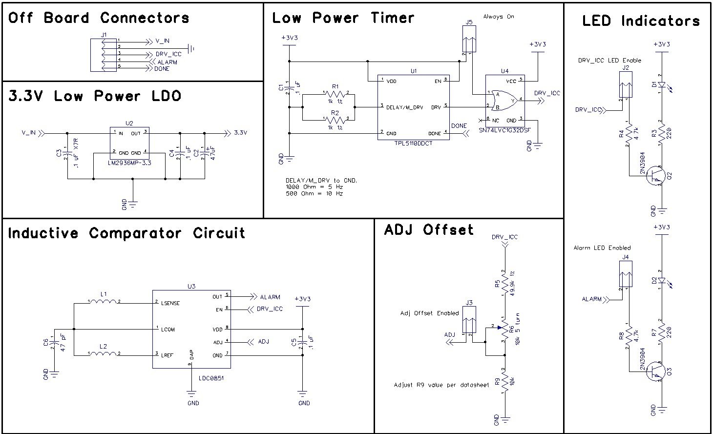
Click to Enlarge Schematic
This circuit makes use of ultra-low power consumption ICs that can function for years on a single button-cell battery. It should be possible to pair this circuit with a Low Power Bluetooth transceiver, such as the CC2640 to create a circuit that can operate for months or years on a single button-cell battery.
There are five off-board connector pins that provide power/ground connections, a signal input, and two signal outputs. The two signal outputs include a heart-beat monitor that indicates each activation of the timer (which can be operated at 5 Hz or 10 Hz), an alarm output that indicates that an inductive target has moved outside of a predetermined range, and a “done” signal input that can be used by a microcontroller to turn off the timer to further conserve energy.
LDC0851 Inductive Switch

The LDC0851 is the main integrated circuit that all other components support. L1 and L2 are the sense and reference coils that, together with C6, create two LC circuits that allow the LDC0851 to detect external events by monitoring changes in inductance. A jumper in conjunction with an OR gate allows the user to place the IC in an always-on state for testing. In normal operation, the sensor will be turned on five or ten times each second by the timer IC; this reduces current consumption.
The coils used in this circuit have an external diameter of 0.750 inches, which provides an estimated switching distance of 0.25 inches. The WEBENCH calculated inductance of each coil is 5.72 µH, and the total capacitance of the LC circuit is approximately 62 pF. Total capacitance is calculated by adding C6, the estimated parasitic capacitance of the board, and the parasitic pin capacitance of the LCOM pin (available in the datasheet).
The operating frequency of the sensor will be approximately 12 MHz, which is safely within the acceptable range of 300 kHz to 19 MHz.
$$f_{sensor}=\frac{\sqrt{2}}{2\pi\sqrt{L_\text{Sensor} C_\text{Total}}}$$
$$f_{sensor}=\frac{\sqrt{2}}{2\pi\sqrt{5.72 \mu\text{H}\cdot 62\text{pF}}}=12 MHz$$

The LDC0851 alternatingly drives each coil through several oscillations and compares the characteristics of the waveforms. The image above depicts the waveforms of each inductive coil (sense and reference) during a transition from driving one coil to driving the other coil, as measured from the center point of each coil. These waveforms were captured with Tektronix TPP1000 probes (3.9 pF) connected to an MDO3104 oscilloscope.
Adjustable Trigger Offset

An optional, adjustable offset is provided to fine-tune the trigger range. It is possible to further increase the range by choosing a different value for R9 according to the table provided in the datasheet.
TPL5110 Low-Power Timer IC

A low-power timer is provided to periodically enable the LDC0851, the voltage divider, and an LED indicator. If you eliminate the LED functionality (by removing J2) and use the timer to enable and disable the LDC0851 circuit, the entire device can operate for several years on a single watch battery.
Two 1 kΩ resistors are connected in parallel with a narrow trace near one side of the circuit board to create a 500 Ω equivalent resistance.

To increase the overall resistance, and thereby decrease the frequency of operation, use a sharp knife to break the narrow trace between R1 and R2. To return to the original resistance, create a solder bridge across the two traces.

Two identical LED indicator circuits are provided for use during testing and adjustment of the circuit. Compared with the rest of the components on the board, they consume a significant amount of power, so don’t use the LEDs if you are trying to maximize battery life.
One LED indicator is wired to the “DRV” output of the timer, and the other is connected to the “alarm” signal of the inductive switch.
Conclusion
“Locks are made for honest people.” This circuit is made for the dishonest ones. Consider it a jumping off point for your next project. Hook it up to an alarm panel, a Bluetooth transmitter connected to your phone, the alarm input on your DVR, or perhaps the bathroom cabinet where you store your prescription medications.
TamperDetectionCircuitv3_DesignFiles.zip
Give this project a try for yourself! Get the BOM.
Related Content


>>perhaps the bathroom cabinet where you store your prescription medications.
It’s generally not OK to store prescriptions in the bathroom with a shower. It’s more fun to fill the medicine cabinet with marbles. Snakes might be a deterrent too, but not my case. A friend had a party and had his 10 foot Boa Constrictor hang out around the medicine cabinet. Snake didn’t bother me and I didn’t go into the medicine cabinet.
Hi
Nice project to watch on a door.
But a simple computation of the power needeed for 1 year :
20µA * 24*365 hours gives 175 mAh
which is not safe at all using a simple CR2032 coin cell of 225 mAh.
Have a look on this reference :
https://www.embedded.com/electronics-blogs/break-points/4429960/How-much-energy-can-you-really-get-from-a-coin-cell-
Energy computation (or simulation with as close as possible to real consumption) is COMPULSORY for autonomous embedded design.
Best regards.
Bernard