 Facebook
 Google
 GitHub
 Linkedin
An Introduction to Switched-capacitor Circuits
In this series of articles, we’ll discuss one of the fundamental building blocks of analog IC design: the switched-capacitor circuit.
One of the most popular approaches for realizing analog signal processing on the IC level is switched-capacitor circuits. Applications for this technology range from filters, AC/DC converters, comparators, telecommunications, and everything in between.
This article will provide an introduction to the field of switched-capacitor circuits, starting with a broad overview and then diving into a fundamental circuit block: the switched-cap resistor.
What Is a Switched-Capacitor Circuit?
A switched-capacitor circuit is a discrete-time circuit that exploits the charge transfer in and out of a capacitor as controlled by switches. The switching activity is generally controlled by well-defined, non-overlapping clocks such that the charge transfer in and out is well defined and deterministic.
These circuits can be thought of as a type of sample and hold circuit, where values are sampled and passed around through the circuit to achieve the desired functionality.
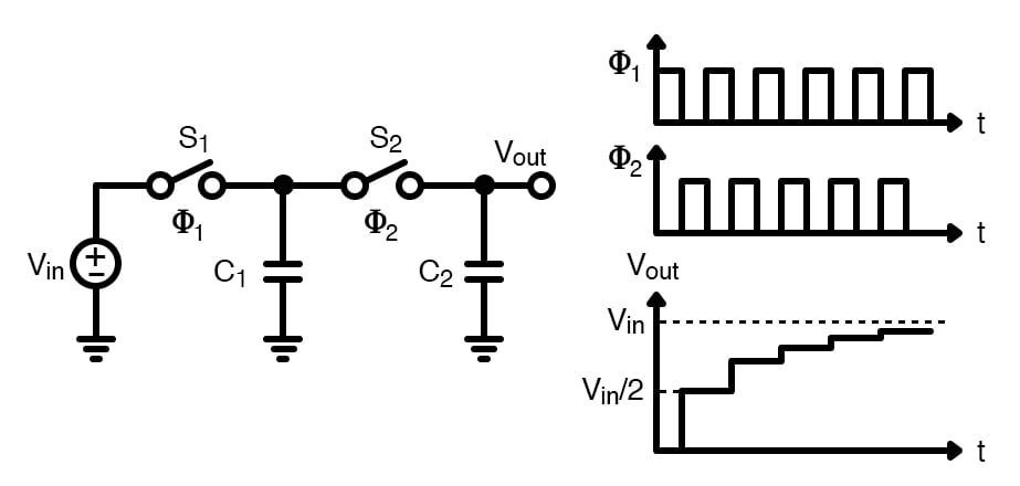
A switched capacitor circuit with non-overlapping clocks. Recreated image used courtesy of Ma et al.
Switched-capacitor circuits are very popular in applications such as filter designs thanks to their extremely accurate frequency response along with good linearity and dynamic range.
As we’ll see later, the discrete time-frequency responses of switched-cap filters are set entirely by the capacitance ratios and the circuit clock frequency, allowing the response to be set precisely on the order of 0.1%. Continuous-time filters, on the other hand, set their frequency response based on RC time constants, where values can vary by as much as 20% due to process variations.
Switched-capacitor Resistor
The most fundamental building block of switched-capacitor circuit design is the switched-capacitor resistor. As mentioned, this circuit has two non-overlapping clocks of the same frequency, ø1 and ø2. To analyze this circuit, we’ll look at two stages.
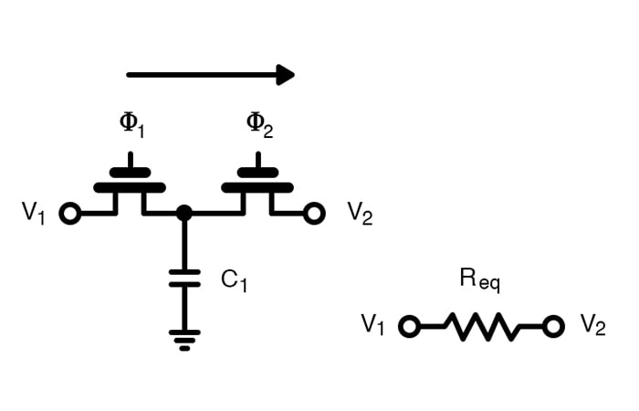
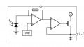
A switched-capacitor resistor. Recreated image used courtesy of Carusone et al.
In the first stage, switch 1 is turned on while switch 2 is turned off. In this setup, the charge flows from node V1 into the capacitor. In the second stage, switch 1 opens while switch 2 is closed. At this point, C1 is connected to node V2 and will either charge or discharge until the final voltage on the capacitor is at V2. The total value of this charge at each stage is given as
\[Q_1 = C_1V_1\]
\[Q_2=C_1V_2\]
If we were to consider the total change in charge, we get the following equations:
\[\Delta Q = C_1(V_1-V_2)=C_1 \Delta V\]
Knowing that current is defined as a change of charge with respect to time and that our change in time is nothing more than our clock period, we can get the average value of current across this switched capacitor:
\[I_{eq} = \frac{C_1(V_1 -V_2)}{T} = C_1 \Delta Vf\]
Finally, we can use the above equation to find the equivalent resistance of the circuit:
\[\mathbf{R_{eq}= \frac {T}{C_1} = \frac {1}{C_1f}}\]
A quick note: I would be remiss not to mention that the previous analysis assumes that the charge transferred per clock cycle is constant over many cycles, allowing us to approximate average currents and resistances. For situations in which the input signal is changing quickly relative to the sampling frequency, a discrete-time z-domain analysis is required.
Area Savings and Controlled Frequency Response
From these results, we can see the magic of switched-cap circuits: they allow designers to create very tightly controlled resistance that depends only on the clock frequency and capacitor value.
One benefit of this technique is that it helps save space. Achieving large resistances generally requires a sizable amount of silicon area. Both factors can be made significantly smaller with switched-cap circuits.
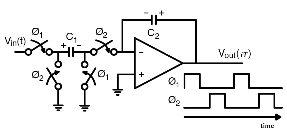
A switched-capacitor integrator with non-overlapping clocks. Recreated image used courtesy of Tenhunen et al.
Another benefit is the fact that mismatch between resistors and capacitors in a continuous-time RC filter is limiting. Matching between similar devices tends to be much better (capacitor to capacitor) as opposed to different devices (capacitor to resistor), making switched-cap filters more precise with their frequency response.
Finally, since our resistance value is set totally by the capacitance value and the frequency, we can dynamically change our filter’s frequency response by changing the clock frequency.
The applications of switched-capacitor circuits are far and wide—and for good reason. Many circuits from filters to ADCs leverage these techniques for their area savings and tightly controlled frequency responses.
Do you have experience designing switched-capacitor circuits? If so, share your experiences in the comments below.
Related Content


Great article and very clear writing thank you for doing such a nice job. A few thoughts…
Switched capacitor circuits have a wide range of use cases from
active filters, PLLs, to charge pumps etc. The are some disadvantages
to keep in mind in practical application of these circuits. Specifically
generating the switching phases of the clocks you need to keep
everything synchronized. You can see from the equations presented
above that any noise/jitter on the switching clock phases will show
up on the Req (Equivalent Resistance) part of the equation. This
will create a moving frequency response as a function of clock phase
noise. If not controlled or accounted for this can make an active filters
frequency response unpredictable.
Also there is always a concern of how these clock phases are generated
and distributed on a PCB or in IC routing. There are noise factors here
due to capacitive and inductive cross-talk that if not carefully accounted
for could lead to unstable behavior in the filter, especially if coupled
to an op-amp in correctly.
From my experience I tend to use charge-pump switched capacitors ICs
like CAT3200TDI from ON Semiconductor. With these devices the timing
generation is all on-chip and as long as you use good routing a lot
of the noise issues are minimized. One hint is to use a little more
input and output capacitance than suggested since capacitors do age.
Use X7R or X5R dielectric capacitors, 0603 case size gives you a nice
range to choose from. Also with a little higher output capacitance the
VOUT probably wont droop as much under a higher load. For the CAT3200
for example the output capacitance is 1uf to 4.7uF which for a 2MHz voltage
doubler is about right. Also you can generate negative voltages easily for
use in your analog op-amp circuits without have to use a regulator or inverting
switcher.
Thank you for the article. There is one single point I like to comment - because I know that some misunderstandings do exist: It is clear that V1 in the switched-capacitor resistor is an applied voltage. But what about V2? Can we connect two such S/C resistors in series and V2 is the voltage between both devices? The answer is NO ! The good functioning of the S/C equivalent requires that V2 is (a) another voltage source or (b) a very large capacitor or (c) V2=0 (ground potential) or (d) virtual ground as for the classical S/C integrator stage.
More than that, it would complete the story about S/C basics when you could show and explain the three different methods for realizing an S/C resistor equivalent: EULER-forward, EULER-backward and BILINEAR.
>One benefit of this technique is that it helps save space. Achieving large resistances generally requires a sizable
amount of silicon area.
This does not make much sense because the capacitors are not usually on the chip. So you are trading off a tiny
metal film resistor for two large and more expensive capacitors.