Facebook
 Google
 GitHub
 Linkedin
Using Verilog to Describe a Sequential Circuit
This article focuses on using Verilog to describe synchronous sequential circuits.
This article focuses on using Verilog to describe synchronous sequential circuits.
In a previous article, we discussed the description of combinational circuits using Verilog language elements. This article focuses on describing synchronous sequential circuits. We’ll first look at a general model for synchronous circuits and then discuss the Verilog description of a bidirectional counter as an example.
Sequential Circuits
In a combinational circuit, the output depends only on the present value of the inputs. However, the output of a sequential circuit depends on not only the current value of the inputs but also the state of the circuit. The state of the circuit is determined by the previous values of the inputs.
Hence, a sequential circuit has memory and its output depends on the sequence of the past inputs. These circuits use memory elements, such as flip-flops (FFs), to store the current state of the system.
Synchronous Sequential Circuits
When dealing with a large sequential circuit, the design problem becomes much more approachable if we use the synchronous methodology rather than asynchronous approach. In a synchronous circuit, all the storage elements are triggered by the same clock signal. This gives us a better control over the system because, in this case, we know when the data is going to be sampled by the storage elements.
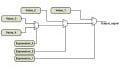
Since all of the storage elements of a synchronous system are connected to the same clock, we can model the system as shown in Figure 1.
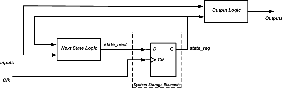
Figure 1
In this model, the dashed box represents all the storage elements of the system ( D-type FFs in this example). The blocks outside the dashed box are combinational circuits.
The “Next State Logic” processes the “Inputs” and the current state of the system, represented by “state_reg”, to determine the next state of the system (“state_next”). With the upcoming rising clock edge, “state_next” will be stored on the FFs. The “Output Logic” block is again a combinational circuit that processes the “Inputs” and “state_reg” to determine the system outputs.
Separating a synchronous system to storage elements and some combinational circuits as shown in Figure 1 helps us to more easily find the HDL description of the system. We only need to describe some combinational circuits and connect them to the memory elements. While, the HDL description of combinational circuits was discussed in a previous article, for the memory elements we usually use some well-known HDL templates.
We’ll look at the Verilog code of a universal counter to clarify these concepts but, before that, we need to take a look at the HDL description of a D-type flip-flop, also known as a DFF.
(For more information on flip-flop bi-stable single-bit memory devices, check out our article on converting D flip-flops into SR, JK, and T flip-flops.)
HDL Description of a Flip-Flop
In general, a DFF can be implemented using the basic logic gates. However, this is not at all recommended when using an HDL to implement a DFF in an FPGA. The safe and efficient method is to describe an FF is using some well-known HDL templates as discussed in the following section. In fact, the synthesis tool recognizes such templates as FFs and uses some optimized structures to implement them.
Verilog Code For a DFF
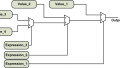
Figure 2 below shows the symbol for positive-edge (Figure 2-a) and negative-edge (Figure 2-b) DFFs. At the clock edge, the input (D) of a DFF is sampled and passed on to the output (Q). For a positive-edge DFF, the sampling edge is the clock rising edge (Figure 2-a) while a negative-edge DFF is sensitive to the falling edge of clock. An FF usually has a reset (rst) that can be used to initialize the system to a known state.
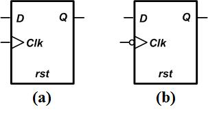
Figure 2
The Verilog code for a positive-edge DFF is given below:
1	module D_FF
2		(
3			input wire clk, reset,
4			input wire d,
5			output reg q
6		 );


7		 always @(posedge clk, posedge reset)
8			if (reset)
9				q <= 1'b0;
10			else
11				q <= d;

12	endmodule
Line 7 of this code uses the “posedge” keyword before the “clk” and “reset” inputs in the sensitivity list of the “always” block. “Posedge”, which stands for positive edge, tells the synthesis tool that the “always” block should be activated at the rising edge of the “clk” and “reset” signals.
Note that the rising edge of both “clk” and “reset” are in the sensitivity list. Hence, a rising edge of “reset” will activate the “always” block irrespective of the “clk” signal condition. In other words, the “reset” of this DFF is asynchronous.
Lines 8 to 11 use the Verilog “if” statement that was discussed in our previous article. When the “always” block gets activated, the “reset” is checked. If it’s logic high, the DFF output is reset (q <= 1’b0). If “reset” is not logic high, then it’s the “clk” signal that has experienced a rising edge and the DFF output should get the value of input (q <= d).
Note that we use non-blocking assignment (<=) when inferring flip-flops. As discussed in another article, improper use of blocking (=) and non-blocking (<=) assignments can lead to undesired functionality. However, for the purpose of this introductory article, we can simply separate the combinational part of the system from its memory elements and follow these two guidelines:
- Use blocking assignments to describe combinational circuits.
- Use non-blocking assignments to infer FFs.
Now, let’s look at the Verilog code of a bidirectional counter to further clarify our discussion.
Verilog Description of a Bidirectional Counter
We’ll write the code for a bidirectional counter that can execute four functions as listed in the following table:
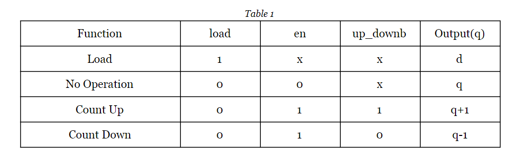
When the “load” input is asserted, the input data (d) is loaded into the counter (q=d). When both “load” and “en” are logic low, the counter keeps its current value. For “load”=0 and “en”=1, the counter may count either upward or downward depending on the value of the “up_downb” input.
The Verilog code for an eight-bit bidirectional counter is given below:
1	module bidirect_cnt8
2		(
3			input wire clk, reset,
4			input wire en, load, up_downb,
5			input wire [7:0] d,
6			output reg [7:0] q
7		);

8		reg [7:0] q_next;

9	// The storage elements
10		always @(posedge clk, posedge reset)
11			if (reset)
12				q <= 8'h00;
13			else
14				q <= q_next;

15	//The next state logic
16		always @*
17			if(load)
18				q_next = d;
19			else if (~en)
20				q_next = q;
21			else if (up_downb)
22				q_next = q + 8'h01;
23			else
24				q_next = q - 8'h01;


25	endmodule
Lines 10 to 14 use the template code discussed in the previous section to add eight DFFs to the design. These are positive-edge DFFs and have an asynchronous reset.
When “reset” is logic high, the value 8’h00 is assigned to “q”. The term 8’h00 denotes an eight-bit number in the hexadecimal base (8’h). The value of this number is given by the two hexadecimal digits after the letter “h”. Hence, when “reset” is logic high, the eight bits of “q” are all set to logic low.
When “reset” is logic low, “q_next” is assigned to “q”. “q_next” represents the output of the “Next State Logic” in the general model of Figure 1 and determines the value that should be assigned to “q” at the upcoming clock rising edge.
Except for lines 10 to 14 that describe the storage elements of the counter, the other lines of the code describe combinational circuitry. Separating storage elements from combinational circuits is not mandatory, but it can help us more easily describe the system. We only need to determine the appropriate value of “q_next” for the upcoming clock edge. Lines 16 to 24 implement the combinational logic for this part of the design, i.e. the “Next State Logic” block of the model in Figure 1. It uses a nested “if” statement to describe the different function of Table 1:
When the “load” input is logic high, the input data (d) is assigned to “q_next”. When “load” is logic low and the counter is not enabled (“en”=0), the counter should keep its current value (“q_next” should be equal to “q”). For “load”=0 and “en”=1, the counter may count either upward or downward depending on the value of the “up_downb” input.
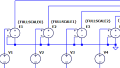
Figure 3 shows an ISE simulation of the code.
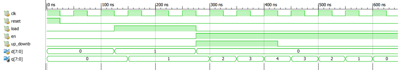
Figure 3
As mentioned above, we do not always have to separate a synchronous system into storage elements and combinational circuits, as in Figure 1. However, I believe this design practice helps us to have a more systematic approach when designing a digital system. In this way, we can more easily visualize a block diagram for the design and find its HDL description.
In this article, we first discussed a general model for synchronous circuits where the system is divided into two parts: storage elements and combinational circuits. Then, we used this model to find the Verilog description of a bidirectional counter. This is not the only way to describe a synchronous system; however, the discussed methodology can simplify the design process.
To see a complete list of my articles, please visit this page.
Related Content