 Facebook
 Google
 GitHub
 Linkedin
Describing Combinational Circuits in Verilog
This article introduces the techniques for describing combinational circuits in Verilog by examining how to use the conditional operator to describe combinational truth tables.
This article introduces the techniques for describing combinational circuits in Verilog by examining how to use the conditional operator to describe combinational truth tables. It also shows how to utilize the Verilog “always” block for describing combinational circuits—an “always” block can provide us with an even easier solution to describe a digital circuit.
In a previous article, we discussed the use of the Verilog “assign” keyword to perform a continuous assignment. Such assignments are always active and can be used to acquire a gate-level description of digital circuits. For example, in the following code, which describes an AND gate, the right-hand side is continuously evaluated and the result is put on the out1 net:
assign out1 = a & b; Verilog has a conditional operator (?:) which allows us to check a condition before making such assignments. The syntax is given below:
assign [signal_name] = [conditional_expression] ? [value_if_true] : [value_if_false];
The “conditional_expression” is evaluated. If it’s true, “value_if_true” is assigned to “signal_name”. If it’s not true, “signal_name” gets “value_if_false”. As an example, consider the following code:
assign out1 = (sel) ? (a & b) : (a|b);If “sel” is true, a&b will be assigned to “out1”. If it’s not true, “out1” will get a|b. Hence, the above code implements the functionality of a 2-to-1 multiplexer. The conceptual implementation of this code can be as shown in Figure 1 below.
The conditional assignment allows us to have a more abstract description of certain circuits because it has the functionality of an “if” statement found in traditional computer programming languages. The conditional operator can be used in a nested form to implement more complex circuits. Example 1 discusses these details.
Example 1: Nested Conditional Operators
Use the conditional operator (?:) to describe a 4-to-2 priority encoder with the following truth table:
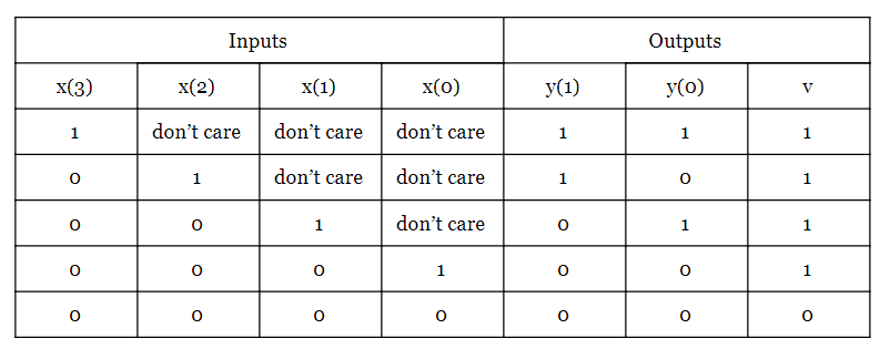
The Verilog code for this priority encoder is given below:
	module Prio_4_to_2
	    (
	    input wire [3:0] x,
	    output wire [1:0] y,
	    output wire v
	    );

	 assign y =  x[3] ? 2'b11 :
		        x[2] ? 2'b10 :
		        x[1] ? 2'b01 :
		       2'b00;

	 assign v = ( x[3] | x[2] | x[1] | x[0] ) ? 1'b1 : 1'b0;

	endmodule
Aside from lines 7 through 10, the code contains the basic language elements discussed in our previous article. So let’s take a look at these lines.
The terms 2’b11, 2’b10, 2’b01 refer to the Verilog notations that represent two-bit binary numbers. In general, the first number (before ‘b) specifies the number of bits. The letter b specifies that the numbers are binary. The digits after ‘b give the value of the number. Hence, 2’b01 is the Verilog notation to represent a two-bit binary number with value 01 and 3’b100 denotes a three-bit binary number with value 100.
Line 7 checks the MSB of the input, x[3], in a conditional operator. If x[3]=1, the condition is evaluated as true and 2’b11 is assigned to y (the assigned value is taken from the truth table). If x[3]=0, the condition is evaluated as false and the expression after the colon (:) will be assigned to y. The expression after the colon is the code in Line 8 which is itself another conditional operator.
The second conditional operator in Line 8 examines the second most significant bit of the input, x[2], to determine whether 2’b10 should be assigned to y or the expression after the colon which is again another conditional operator (Line 9) should be evaluated. You can verify that the values assigned to y match the given truth table.
The valid output (v) of the truth table will be logic high if at least one bit of the input is logic high. Line 11 shows this description by applying the bitwise OR operator (|) to the bits of the input. A Xilinx ISE simulation of the above code is shown in Figure 2.
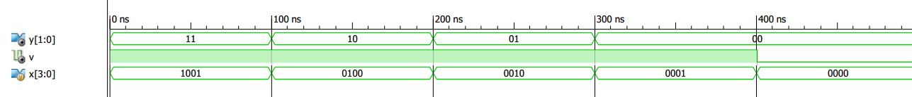
Figure 2. A Xilinx ISE simulation from the above code.
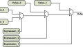
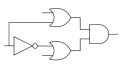
It’s important to note that the conditional expressions are evaluated successively until a true expression is found. The assignment corresponding to this true expression will be performed. As a result, the expressions evaluated earlier have a higher priority in comparison to the next ones. This means that, theoretically, a conditional operator is more suitable for implementing a priority network (Figure 3) rather than a balanced structure such as a multiplexer (Figure 4).
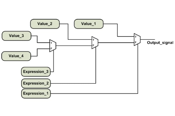
Figure 3. A priority network.
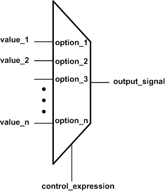
Figure 4. An n-to-1 multiplexer wherein there’s no priority between the inputs.
A previous article reveals a similar discussion about VHDL concurrent assignments.
Verilog Procedural Statements
We can pull apart any combinational circuit into a few basic logic gates (AND, OR, NOT, etc.) and use the “assign” statement to describe these gates (a gate-level description). We can also use the conditional operator discussed in the previous section to have a more abstract way of describing some combinational circuits (similar to the “if” statement of computer programming languages). However, there’s still a more powerful solution: using the Verilog “always” block.
Inside an “always” block, we can have procedural statements that are executed in sequence. Moreover, the “always” block supports abstract language constructs such as “if” and “case” statements.
The sequential execution feature along with the abstract language constructs available within an “always” block allows us to more easily describe the functionality of a circuit, due to the fact that human reasoning has a sequential nature and relies on abstract descriptions. We usually think in an algorithmic high-level fashion rather than in terms of low-level logic gates. An “always” block can provide us with an easier solution to describe a digital circuit. For more details about why HDLs support descriptions based on sequential statements, please see my article Introduction to Sequential VHDL Statements.
Example 2: "Always" Block Statements
The simplified syntax of an “always” block is given below:
always @(sensitivity_list)
	begin
		sequential_statements;
	end
The sensitivity_list specifies when the sequential statements inside the “always” block should be executed. For example, consider using the “always” block to describe the circuit in Figure 5.
.png)
Figure 5. Circuit_1
When either a or b changes the output may change, which means both a and b should be in the sensitivity list of the “always” block. In general, for a combinational circuit, all the input signals should be included in the sensitivity list.
Now, we can use the bitwise AND operator to describe the functionality of the circuit (a&b) and assign the result to the output. Within an “always” block, there are two different types of assignments: the blocking assignment (=) and the non-blocking assignment (<=). Using the blocking assignment, we obtain the following code:
always @(a, b)
begin
     out1 = a & b;
end
What’s the difference between a blocking assignment and a non-blocking assignment?
With a blocking assignment, the right-hand side is evaluated and immediately assigned to out1. Hence, when Line 3 is executed, out1 gets immediately updated before we go to the next line of the code. The name “blocking assignment” emphasizes that the upcoming lines are blocked until the left-hand side gets updated.
With a non-blocking assignment, the right-hand expression is evaluated but it’s not applied to the left-hand variable until we reach the end of the “always” block. The choice of blocking or non-blocking assignment can be confusing for a beginner and improper use of them can lead to an undesired functionality. For example, using blocking assignments to infer flip-flops may introduce a race condition.
For this introductory article, we won’t further go into details and we’ll only stick to one simple guideline to avoid potential pitfalls: Use the blocking assignments when writing the code for a combinational circuit. Hence, the “always” block in Listing 1 will be used to describe an AND gate.
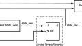
In a previous article, we got familiar with the Verilog “wire” data type. This data type represents a physical wire in our FPGA design. Within an “always” block, the Verilog standard doesn’t allow us to assign a value to a “wire”. Instead, we use the “reg” data type. The name “reg” is somewhat confusing, but note that a “reg” may or may not lead to a physical storage element in your design. The following code is the Verilog description of Figure 5 using an “always” block. Note that the output data type should be “reg” because it gets its value from a procedural assignment.
	module Circuit_1
	    (
	    input wire a,
	    input wire b,
	    output reg out1
	    );

		 always @ (a, b)
		 begin
			out1 = a & b;
		 end

	endmodule
In this article, we got familiar with the Verilog conditional operator. We used the nested form of this operator to describe a priority encoder. Then, we touched on a more powerful language construct, the “always” block, to describe combinational circuits. In future articles, we’ll examine the use of the “always” block to implement sequential circuits.
Related Content


Nice article, always a pleasure to read combinational logic instead of combinatorial logic! Just a couple comments that expand a little on the material presented and may be useful for the target audience.
Instead of writing:
assign v = ( x[3] | x[2] | x[1] | x[0] ) ? 1’b1 : 1’b0;
many will prefer:
assign v = ( |x[3:0] ) ? 1’b1 : 1’b0;
or simply:
assign v = |x;
Some may consider the first version more readable and explicit, while others may consider it verbose and pedantic. Eye of the beholder. If you’re generating parity for a wide data path it’s definitely a time saver to write:
assign p = ^d;
It seems worth mentioning that in addition to an explicit sensitivity list, today’s Verilog tools support a wild card:
always @ (*)
This means the left-hand side will evaluate whenever any right-hand side variable changes, the correct behavior for a combinational logic block.
The wild card has the benefit of not requiring a co-requisite sensitivity list change if the right-hand side is modified, and also of not being susceptible to inadvertently omitting a variable from the sensitivity list which can result in latch inference and obscure bugs that may not readily appear depending on test coverage.