 Facebook
 Google
 GitHub
 Linkedin
Edge-triggered Latches: Flip-Flops
So far, we’ve studied both S-R and D latch circuits with enable inputs. The latch responds to the data inputs (S-R or D) only when the enable input is activated. In many digital applications, however, it is desirable to limit the responsiveness of a latch circuit to a very short period of time instead of the entire duration that the enabling input is activated.
One method of enabling a multivibrator circuit is called edge triggering, where the circuit’s data inputs have control only during the time that the enable input is transitioning from one state to another.
Let’s compare timing diagrams for a normal D latch versus one that is edge-triggered:

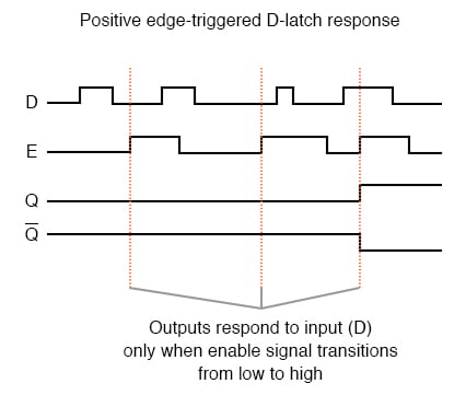
In the first timing diagram, the outputs respond to input D whenever the enable (E) input is high, for however long it remains high. When the enable signal falls back to a low state, the circuit remains latched.
In the second timing diagram, we note a distinctly different response in the circuit output(s): it only responds to the D input during that brief moment of time when the enable signal changes, or transitions, from low to high. This is known as positive edge-triggering.
There is such a thing as negative edge triggering as well, and it produces the following response to the same input signals:

Whenever we enable a multivibrator circuit on the transitional edge of a square-wave enable signal, we call it a flip-flop instead of a latch.
Consequently, and edge-triggered S-R circuit is more properly known as an S-R flip-flop, and an edge-triggered D circuit as a D flip-flop. The enable signal is renamed to be the clock signal. Also, we refer to the data inputs (S, R, and D, respectively) of these flip-flops as synchronous inputs, because they have effect only at the time of the clock pulse edge (transition), thereby synchronizing any output changes with that clock pulse, rather than at the whim of the data inputs.
But, how do we actually accomplish this edge-triggering? To create a “gated” S-R latch from a regular S-R latch is easy enough with a couple of AND gates, but how do we implement logic that only pays attention to the rising or falling edge of a changing digital signal?
What we need is a digital circuit that outputs a brief pulse whenever the input is activated for an arbitrary period of time, and we can use the output of this circuit to briefly enable the latch. We’re getting a little ahead of ourselves here, but this is actually a kind of monostable multivibrator, which for now we’ll call a pulse detector.

The duration of each output pulse is set by components in the pulse circuit itself. In ladder logic, this can be accomplished quite easily through the use of a time-delay relay with a very short delay time:

Implementing this timing function with semiconductor components is actually quite easy, as it exploits the inherent time delay within every logic gate (known as propagation delay). What we do is take an input signal and split it up two ways, then place a gate or a series of gates in one of those signal paths just to delay it a bit, then have both the original signal and its delayed counterpart enter into a two-input gate that outputs a high signal for the brief moment of time that the delayed signal has not yet caught up to the low-to-high change in the non-delayed signal. An example circuit for producing a clock pulse on a low-to-high input signal transition is shown here:

This circuit may be converted into a negative-edge pulse detector circuit with only a change of the final gate from AND to NOR:

Now that we know how a pulse detector can be made, we can show it attached to the enable input of a latch to turn it into a flip-flop. In this case, the circuit is a S-R flip-flop:

Only when the clock signal (C) is transitioning from low to high is the circuit responsive to the S and R inputs. For any other condition of the clock signal (“x”) the circuit will be latched.
A ladder logic version of the S-R flip-flop is shown here:

Relay contact CR3 in the ladder diagram takes the place of the old E contact in the S-R latch circuit and is closed only during the short time that both C is closed and time-delay contact TR1 is closed. In either case (gate or ladder circuit), we see that the inputs S and R have no effect unless C is transitioning from a low (0) to a high (1) state. Otherwise, the flip-flop’s outputs latch in their previous states.
It is important to note that the invalid state for the S-R flip-flop is maintained only for the short period of time that the pulse detector circuit allows the latch to be enabled. After that brief time period has elapsed, the outputs will latch into either the set or the reset state. Once again, the problem of a race condition manifests itself. With no enable signal, an invalid output state cannot be maintained. However, the valid “latched” states of the multivibrator—set and reset—are mutually exclusive to one another. Therefore, the two gates of the multivibrator circuit will “race” each other for supremacy, and whichever one attains a high output state first will “win.”
The block symbols for flip-flops are slightly different from that of their respective latch counterparts:

The triangle symbol next to the clock inputs tells us that these are edge-triggered devices, and consequently that these are flip-flops rather than latches. The symbols above are positive edge-triggered: that is, they “clock” on the rising edge (low-to-high transition) of the clock signal. Negative edge-triggered devices are symbolized with a bubble on the clock input line:

Both of the above flip-flops will “clock” on the falling edge (high-to-low transition) of the clock signal.
REVIEW:
- A flip-flop is a latch circuit with a “pulse detector” circuit connected to the enable (E) input, so that it is enabled only for a brief moment on either the rising or falling edge of a clock pulse.
- Pulse detector circuits may be made from time-delay relays for ladder logic applications, or from semiconductor gates (exploiting the phenomenon of propagation delay).
RELATED WORKSHEETS:


On the positive/negative edge triggered symbols for the SR flip flops, what does the bubble by Q’ mean? Doesn’t this just make the both outputs equivalent to Q, so they will both have the same timing diagrams? ie. not Q’ = Q.
I was looking for this all over the internet without any luck. Finally got this article which explains how clock signals can made to function at the edge signals only. Thanks to all the authors and contributors