Facebook
 Google
 GitHub
 Linkedin
How Neuromorphic Chips are Revolutionizing the Edge
Neuromorphic Edge AI chips mark a fundamental departure from traditional silicon, utilizing brain-inspired, event-driven architectures to enable real-time inference within milliwatt-level power budgets.
By integrating raw sensory acquisition and local compute within a single chip, these designs provide an efficient path for augmenting existing hardware. Developers can now upgrade legacy SoCs and microcontrollers with advanced AI capabilities without the need for a costly and time-consuming system redesign.
Figure 1. Neuromorphic AI chip with advanced technology. Image used courtesy of Adobe Stock (licensed).
This modular approach is particularly transformative for next-generation wearables, medical implants, and remote industrial sensors, where strict heat constraints and device longevity are primary barriers to innovation and adding power hungry add-on chips often cannot meet these constraints.
Enter neuromorphic compute solutions, which provide a scalable, low-latency pathway for deploying sophisticated machine learning in environments where traditional NPU-based AI is physically or economically unfeasible.
By processing data locally at the source, these chips eliminate bandwidth bottlenecks and privacy concerns associated with cloud-reliant intelligence, bringing high-performance AI to the most resource-constrained IoT environments. By utilizing neuromorphic compute principles, the NPU only consumes power when meaningful information triggers the activation functions for latter layer processing, saving significant compute and also reducing latency.
Unlocking Efficiency Through Event-Driven Processing
Neuromorphic accelerators—primarily utilizing Spiking Neural Networks (SNNs)—remain in a near-idle state until a specific stimulus is detected, unlike standard processors that rely on constant compute cycles. This model ensures energy is only consumed during active computation, mimicking the biological efficiency of the human brain.
This event-triggered execution allows for complex pattern recognition at the extreme edge, which is critical for "always-on" applications monitoring environments for extended periods. The result is a highly responsive system that provides high-fidelity diagnostic data without the thermal penalties or battery requirements of conventional architectures.
Furthermore, this approach optimizes data flow by processing only changes in sensory input rather than redundant signals. In vision or vibration sensors, the network can ignore static background signals to focus exclusively on dynamic events. This inherent efficiency prioritizes critical information and extends device longevity in battery-limited edge nodes.
Augmenting Legacy Hardware with Seamless Integration
These processors offer a streamlined route for enhancing current hardware, enabling complex data processing without typical power penalties. Rather than forcing a 'rip-and-replace' strategy, this model facilitates a strategic evolution of current platforms, bridging the gap between traditional embedded design and next-generation intelligence.
Instead of replacing entire architectures, neuromorphic co-processors act as an intelligent "sensory layer" that offloads AI workloads from the main processor. This allows the primary MCU or MPU to remain in deep-sleep mode until the neuromorphic chip triggers an interrupt based on a high-confidence event. By preserving the existing software stack, manufacturers can significantly reduce R&D overhead and accelerate time-to-market.
Moreover, this integration model broadens access to sophisticated machine learning at the network's most constrained edge. The transition to AI-enabled hardware becomes a scalable operational upgrade rather than a risky infrastructural overhaul, ensuring that even power-sensitive devices can participate in the modern AIoT ecosystem.
A Scalable Solution for Resource-Constrained Environments
The true scalability of neuromorphic technology lies in maintaining high computational throughput within the rigid physical footprints of edge devices. Unlike conventional AI accelerators that require bulky thermal management, these chips operate with minimal heat dissipation, allowing for dense intelligence in miniaturized enclosures like topical skin monitors or sealed industrial probes.
From an operational standpoint, this technology enables a decentralized intelligence model that thrives in connectivity-sparse environments. By shifting pattern recognition from the cloud or a remote box to the silicon itself, this autonomy eliminates the power and privacy burden of high-bandwidth uplinks, transforming passive sensors into self-sufficient diagnostic nodes that operate for years on minimal energy.
Additionally, the architectural flexibility of these accelerators allows for a seamless transition across hardware tiers, from basic microcontrollers to advanced integrated systems. As the demand for "always-on" security and predictive maintenance grows, the ability to deploy AI without an economic or energetic overhaul becomes a significant competitive advantage that future-proofs existing IoT deployments.
Redefining the Edge: Real-World Impact
The shift toward brain-inspired silicon marks the end of the era where high-performance AI required high power consumption. By moving beyond traditional constraints, neuromorphic technology enables sophisticated intelligence at the extreme edge. This evolution represents a fundamental transition toward a decentralized digital ecosystem where sensors become active, self-sufficient participants.
By enabling local decision-making, these chips pave the way for devices that are inherently more responsive, private, and energy efficient. This autonomy is a critical enabler for industrial and medical IoT applications where uncompromising reliability is non-negotiable. This localized approach eliminates the bandwidth bottlenecks and security and privacy risks that have traditionally hindered large-scale AIoT deployments.
As we address challenges in data privacy, latency, and sustainability, neuromorphic solutions offer a mature and scalable roadmap. The ability to enhance legacy hardware through seamless integration ensures this technological leap is accessible and rapidly deployable across diverse sectors. Ultimately, event-driven processing is a strategic commitment to autonomous decision-making exactly where it is needed: at the data source.
BrainChip: AKD1500 Neuromorphic Edge AI Accelerator Co-Processor Chip
BrainChip has introduced the AKD1500, a neuromorphic edge AI co-processor designed to provide high-performance artificial intelligence for power-sensitive devices. Built on an event-based digital architecture, the chip mimics the human brain by processing data only when specific "spikes" occur, which significantly reduces energy waste. This makes it an ideal solution for upgrading existing systems in industrial, consumer, and medical sectors without requiring a complete hardware overhaul.
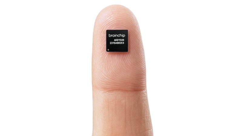
Figure 2. BrainChip’s AKD1500 Edge AI Co-Processor. Image used courtesy of BrainChip.
The co-processor is particularly effective for battery-operated and thermally constrained environments, such as medical wearables for seizure prediction or smart sensors for industrial monitoring. Its versatility allows it to integrate seamlessly with various host platforms like ARM, x86, and RISC-V through standard interfaces. By handling complex tasks locally, the AKD1500 allows larger system processors to remain in low-power states, enhancing the overall energy efficiency of the device.
One of the standout features of the AKD1500 is its capacity for on-chip learning, enabling devices to adapt to new data patterns in real-time without needing cloud-based retraining. This "one-shot" learning capability ensures data privacy and reduces latency, which is critical for healthcare and defense applications. Developed using GlobalFoundries' 22nm process, the chip is scheduled for volume production in the third quarter of 2026.