 Facebook
 Google
 GitHub
 Linkedin
Closed-Loop Control for an LTspice Switching Regulator
Learn how to simulate a switching voltage regulator with a voltage-controlled PWM waveform in LTspice.
My recent articles used LTspice circuit simulations to explore the functionality and performance of different switching regulator topologies. These articles focused on the power stage, which contains the basic components that work together to convert an input voltage into a higher or lower output voltage.
However, a power stage only becomes a true regulator when it’s combined with control circuitry. This control circuitry helps to maintain a specified output voltage by monitoring VOUT and adjusting the duty cycle or frequency of the signal that controls the switch. The output voltage is fed back into the regulator and used to adjust a signal that influences the magnitude of the output. When I refer to closed-loop control, this is what I mean.
In this article, I’ll explain how to simulate closed-loop control in LTspice. Then I’ll demonstrate its application with an LTspice buck converter.
Creating Variable Duty Cycles in LTspice
Each simulation in my previous articles included a pulse-width-modulated (PWM) voltage waveform that controlled the converter’s switch, thereby influencing the magnitude of the output voltage relative to the input voltage. However, the pulse width in these simulations was modulated only on a run-by-run basis. Since the duty cycle was specified via a .param statement, it had to remain constant for the entirety of each simulation run.
I added a bit more modulation into the pulse width by using a .step parameter to create a list of duty cycles that would be applied sequentially during a multi-run simulation, but that’s still a long way from a truly variable duty cycle that would allow us to perform advanced, dynamic analysis of switching regulators.
It is possible to create a voltage-controlled or time-dependent duty cycle in LTspice, though a bit of creativity is required. The duty cycle of the Pulse voltage-source function is determined by the TPERIOD and TON fields, where:
- TPERIOD = the period of the repeating waveform.
- TON = the ON (high) time during each period.
For example, a 1 kHz square wave with 30% duty cycle would have a TPERIOD of 1.0 ms and a TON of 0.3 ms.
Whether you input the numbers directly or use .param statements for convenience, these values are basically hard-coded into the simulation run.
Because of this, we can’t generate a dynamically variable duty cycle directly from a voltage source. Instead, we do so within the simulation, using multiple sources and a comparator.
Signal Implementation
The LTspice functional block in Figure 1 conveys my method of creating a PWM signal for a variable duty cycle simulation.
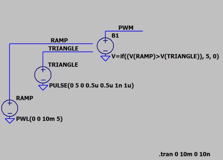
Figure 1. An LTspice functional block for creating a variable PWM signal.
Let’s briefly look at some features of the schematic.
Ramp and Triangle
The RAMP signal increases linearly from 0 to 5 V during the simulation interval. The interval in this case is 10 ms, but you can freely modify it according to your needs.
The TRIANGLE signal increases and decreases linearly between 0 and 5 V at a frequency of 1 MHz. I create a triangle wave by using the Pulse function with negligible on-time and with rise and fall times equal to half of the period.
Behavioral Voltage Source
B1 is an arbitrary behavioral voltage source. The output of an arbitrary behavioral voltage source is determined by a customized function, which in this schematic can be translated as follows: If the voltage of the ramp signal is greater than the voltage of the triangle signal, set B1’s voltage to 5 V; otherwise, set B1’s voltage to 0 V. Essentially, B1 functions as an idealized comparator.
Arbitrary behavioral voltage sources are identified as B sources in LTspice. You can find the component I used by searching for “bv” in the main LTspice library.
Maximum Timestep
If no maximum timestep is specified for this simulation, LTspice chooses a value that creates unacceptably long rise and fall times, resulting in a greatly distorted PWM signal. To avoid this, I included 10 ns as the maximum timestep in the .tran simulation command (.tran 0 10m 0 10n).
A maximum timestep of 10 ns produces crisp waveforms and doesn’t seriously lengthen the simulation time. On my computer, it took about 2.5 seconds to run the simulation with the default timestep and 5 seconds to run it with a 10 ns timestep.
Basic Circuit Operation
The configuration shown above produces a PWM waveform whose duty cycle varies steadily from 0% to 100% over the course of 10 ms. The fundamental mode of action in this circuit can be seen in Figure 2.
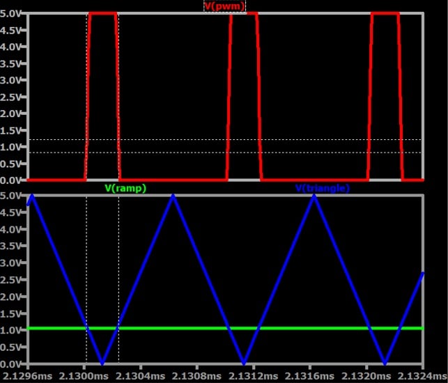
Figure 2. Top plot: Pulse-width-modulated voltage. Bottom plot: ramp voltage (green) and triangle voltage (blue).
Because the ramp signal changes much more slowly than the triangle signal does, the ramp voltage is stable during one period of the triangle wave. The portion of the triangle trace that is below the ramp trace corresponds to the logic-high portion of the PWM signal, and the portion of the triangle trace that is above the ramp trace corresponds to the logic-low portion of the PWM signal.
For this reason, the duty cycle is low at the beginning of the simulation interval. As the ramp voltage gradually increases, so does the logic-high time, until the duty cycle approaches 100% at the end of the simulation interval. This progression from low duty to high duty cycle is shown below in Figures 3, 4, and 5. Note the values on the horizontal axes relative to the 10 ms simulation intervals.
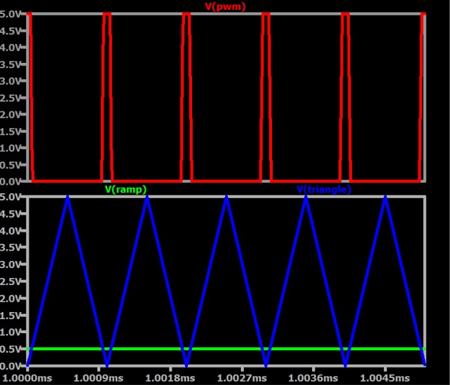
Figure 3. Voltage-controlled circuit behavior at a low duty cycle.
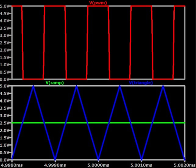
Figure 4. Voltage-controlled circuit behavior at a medium duty cycle.
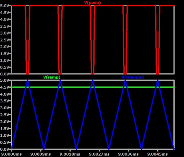
Figure 5. Voltage-controlled circuit behavior at a high duty cycle.
The frequency of the PWM signal equals the frequency of the triangle wave, and the mathematical relationship between the ramp, the triangle, and the duty cycle (D) is straightforward: D is equal to the ramp voltage at a given moment divided by the maximum voltage of the triangle signal.
$$D=\frac{V_{RAMP,\ INSTANTANEOUS}}{V_{TRIANGLE,\ MAX}}$$
This formula assumes that the triangle signal’s minimum voltage is 0 V and that the ramp signal does not extend below 0 V.
This relationship is particularly evident in Figure 4, where the ramp signal is at 2.5 V. Since 2.5 V is 50% of the triangle wave’s maximum voltage, the PWM duty cycle is 50%.
Time-Dependent vs. Voltage-Controlled PWM
The circuit presented in this article remains effective with a control waveform that varies in an irregular or unpredictable fashion. This is the type of waveform that I have in mind when I use the term voltage-controlled. It’s also the type of waveform that we would expect as feedback from a voltage regulator’s output node.
Strictly speaking, our circuit always produces a voltage-controlled PWM signal. We can achieve the equivalent of a time-dependent PWM signal, however, by specifying a control voltage that varies in a simple and consistent way relative to time, such as VRAMP.
Next, we’ll use voltage-controlled PWM to improve the VOUT accuracy of a buck converter.
Creating an LTspice Buck Converter With Closed-Loop Control
Figure 1 contains a combination of voltage sources that will allow us to change the duty cycle of a rectangular wave during a simulation run. When we integrate this functional block with an LTspice buck converter, the feedback will help the actual output voltage converge on the desired output voltage.
If we can use a voltage to control the PWM duty cycle, we have satisfied the fundamental requirement for creating a closed-loop switching regulator circuit. Please note, however, that the circuit we’re creating is for demonstration and instructional purposes only. It doesn’t replicate the details of any real-life switched-mode power supply (SMPS) control circuit.
Additionally, several numerical values in the schematic were chosen based on previous experience and tweaked using trial and error. They aren’t the result of a mathematically rigorous design procedure, and they haven’t been thoroughly optimized.
Schematic and Design
The LTspice schematic in Figure 6 shows a buck converter power stage combined with the voltage sources from Figure 1. Later on, we’ll use this schematic to run simulations.
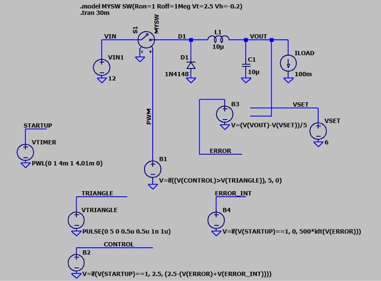
Figure 6. LTspice implementation of a buck converter with closed-loop control.
Let’s briefly go over the functional blocks in the new schematic.
- VTRIANGLE: This voltage source generates a triangle wave that serves as the basis for the PWM waveform.
- VTIMER: This generates a voltage that causes other sources to alter their behavior after a specified length of time, in this case 4 ms.
- B2: This generates the control voltage (VCONTROL) that is compared to VTRIANGLE by voltage source B1 to generate the variable PWM signal.
- B3: This source generates the error voltage. It’s produced by subtracting the desired output voltage (VSET) from the actual output voltage (VOUT).
- B4: This voltage source creates an output voltage that is the integral of the error voltage with respect to time. It’s generated using LTspice’s idt() function.
Circuit Behavior
The objective here is to reduce a 12 V input to a 6 V output. The theoretical duty cycle for a buck converter is D = VOUT/VIN. The circuit therefore has an initial duty cycle of 50%.
To produce a 50% duty cycle, the control voltage (B2) must start at 2.5 V. However, because I want to see the output voltage obtained with and without feedback on the same plot, I set VTIMER so that the converter will operate in open-loop mode for the first 4 ms of our simulation and in closed-loop mode thereafter. When closed-loop operation commences, the control voltage will change.
The aim of closed-loop control is to help VOUT converge on VSET. To achieve this, the circuit modifies the control voltage in response to both the error voltage (which, as mentioned previously, is the difference between VOUT and VSET) and its integral. For information on the purpose of an integral signal in closed-loop systems, please refer to my article on PID control.
Now, without further ado, let’s run our simulation.
Simulation Results
Figure 7 illustrates the circuit’s operation.
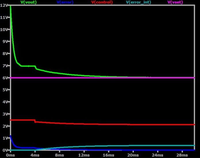
Figure 7. Operation of the buck converter in Figure 6. Initial VOUT is greater than VSET.
Open-loop operation (with 50% duty cycle) results in VOUT = 7 V. The output voltage begins to decrease toward the desired value at t = 4 ms, which is when closed-loop control kicks in. The error voltage causes an initial step downward, which reduces the error voltage in turn. Once this occurs, the integral of the error voltage helps the output voltage to continue approaching the set voltage.
If I change the load current to 1000 mA, the open-loop output voltage drops to about 4.7 V. Figure 8 shows that the circuit functions similarly when VOUT needs to increase, rather than decrease, toward the set voltage.
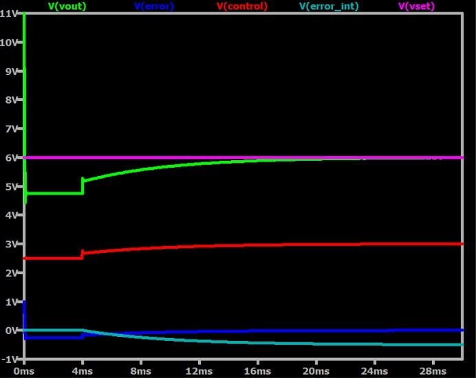
Figure 8. Operation of the buck converter in Figure 6. Initial VOUT is less than VSET.
Wrapping Up
I hope that this article has given you some insight into the use of closed-loop control for switch-mode voltage regulation, and perhaps expanded your repertoire of LTspice techniques. I think that this circuit could be a good starting point for developing more sophisticated or extensive SMPS simulations. If you happen to do that, please leave a comment and tell us what you’ve learned.
All images used courtesy of Robert Keim


Can you please send us the LTSpice schematics file
This article is awesome!! I’ve forever wanted an easy way to make a Voltage controlled PWM in LT. Yes please attach the .asc file so we can be sure to sim exactly what’s in the article.
Where can i find the LTspice files for this simulation?