 Facebook
 Google
 GitHub
 Linkedin
Design Considerations for Digital VLSI
In this article, we discuss metastability, setup time, and hold time in designing a digital VLSI circuit.
Design procedures in VLSI SoCs are very complex. The designer should consider all possible states and inputs and design the chip in such a way that it works every time in every state and with every possible input. In this article, we discuss metastability, setup time, and hold time when designing a digital VLSI circuit.
Critical Path, Throughput, and Latency
The critical path is the longest path in the circuit and limits the clock speed. When describing a digital circuit there are two other important factors: latency and throughput. Latency is the time needed for an input change to produce an output change; latency can be expressed as a length of time or, in synchronous circuits, as a certain number of clock cycles. Throughput refers to the rate at which data can be processed.
Flip-Flops and Combinational Logic
A digital circuit can consist of sequential logic and combinational logic. Sequential logic refers to circuits whose output depends on previous states. In other words, it involves memory that stores previous states and allows a decision to be made based on these previous states and the current input signals. In the digital realm, flip-flops are the standard devices used for storing previous logic states. In Verilog, we can define a flip-flop by using the reg command:
reg[7:0] states;
The above line defines an 8-bit flip-flop. Flip-flops, which are sensitive to clock transitions rather than clock logic states, are the most basic element of synchronous designs.
Combinational logic refers to a circuit that computes an output based only on the current input signals.
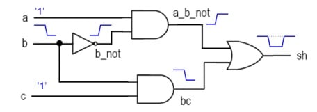
Figure 1. sh = ab’+bc. Image courtesy of the Tampere University of Technology
A simple combinational logic circuit is implemented in Figure 1. Every logic device has a propagation delay. Propagation delay is the time difference between an input change and the corresponding output change. This delay can lead to unexpected behavior, such as when a gate accepts two inputs that come from paths with different numbers of gates (and therefore unequal total propagation delay).
Assume we are in the (1,1,1) input state and the output is steady at 1. If b changes from 1 to zero the output of the lower AND gate will transition before that of the upper AND gate, resulting in a temporary logic low on the output. This logic-low state is invalid, because a (1,0,1) input pattern should produce a logic-high output. This brief invalid output state is referred to as a hazard.
More specifically, this glitch is called a static hazard. Dynamic hazards occur when an input change leads to more than one output glitch. Usually, dynamic hazards occur in complex circuits with multiple gates and logic paths.
In synchronous design, we must ensure that glitches do not result in invalid output states. As mentioned above, for storing previous states designers usually use flip-flops with edge sensitivity. When using flip-flops in digital VLSI designs, we must consider the following:
- Setup time: the input to a flip-flop should be stable for a certain amount of time (the setup time) before the clock transitions; otherwise, the flip-flop will behave in an unstable manner, referred to as metastability.
- Hold time: the input of a flip-flop should remain stable for a certain amount of time (the hold time) after the clock transitions.
The following figure provides a visual description of setup time and hold time:
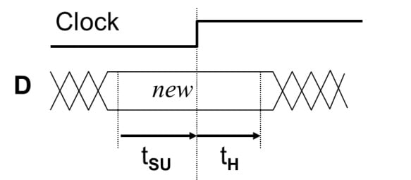
Figure 2. Setup and hold time definitions. Image courtesy of the Tampere University of Technology
Setup Time
A digital circuit designed for FPGA or ASIC purposes needs combinational logic for calculations. We usually build multipliers, subtractors, adders, etc., with logic gates. For storing input and output values for these combinational logic circuits, we use flip-flops. Flip-flops are at the beginning and at the end of all critical paths, as shown in Figure 3.
To avoid a setup-time violation when using flip-flops at the end of a combinational path, the output must be stable before the clock edge. Thus, the total propagation delay of a combinational path must not cause the output to transition such that the relationship between the clock signal and the data signal leads to a setup-time violation.
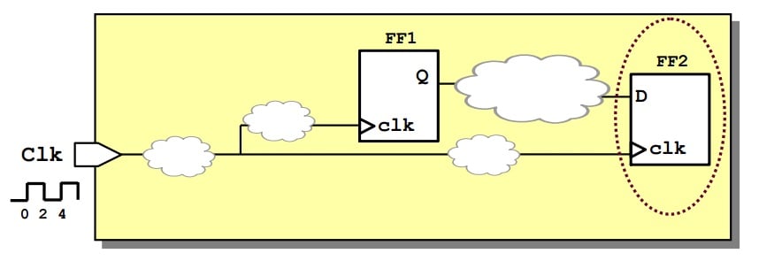
Figure 3. An example of a synchronous digital circuit.
Pipelining
In VLSI designs, we may face a very long critical path due to an extensive combinational circuit. In such cases, our clock speed will decrease to ensure that the delays associated with the critical path do not lead to setup-time violations. Pipelining is a technique whereby we divide a combinational path into multiple parts and include a register at the end of each partial path. In this way, we divide the critical path into multiple small paths, and this allows us to increase the clock speed and, consequently, the throughput of the circuit.
For example, in Figure 4 we have a long critical path that limits the clock frequency. However, the divided and pipelined path (see Figure 5) contains shorter combinational paths, and this means we can increase the clock speed. However, as a trade-off, the latency of the path will increase.
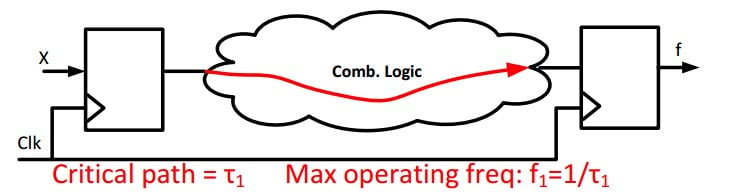
Figure 4. Long combinational logic path. Image courtesy of the Sharif University of Technology (PDF)
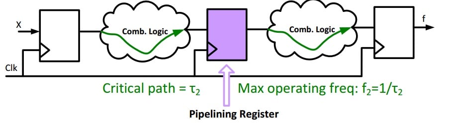
Figure 5. Pipelining of Figure 4 circuit. Image courtesy of the Sharif University of Technology (PDF)
Hold Time
The input to a flip-flop should be stable for an amount of time equal to or greater than the hold time. For example, in Figure 6, assume the delay of the combinational path between FF1 and FF2 is 0.7ns, the flip-flop setup time is 2ns, and its hold time is 1ns. If we assume that the propagation delay of the flip-flops is zero, after a clock edge the output of FF1 will change immediately, and 0.7ns later the signal has passed through the combinational logic and arrived at the FF2 input. However, the input to FF2 should be stable for at least 1ns after the clock edge. Thus, a hold-time violation occurs.
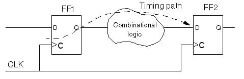
Figure 6. Hold-time violation example. Image courtesy of the VLSI Expert Group
A setup-time violation can be addressed by reducing the clock frequency, even after device fabrication has occurred; however, a hold-time violation cannot be corrected if it is discovered after the fabrication process. The important thing is to design our circuit so that hold-time violations will not occur; a combinational circuit connected to a flip-flop input should have a propagation delay that is compatible with the hold-time requirement.
One technique for avoiding hold-time violations is to increase the delay of a fast path by adding buffers. Nowadays, CAD tools can help by identifying portions of a design that could experience hold-time or setup-time violations. Furthermore, CAD tools can take timing requirements into account when synthesizing, placing, and routing a particular design.
Clock-Crossing
In most modern designs, multiple clock frequencies are used. ADCs or DACs may have a clock that is not synchronized with the FPGA clock, and yet the ADC or DAC signals must be introduced into the FPGA clock domain. When we're working with multiple clock domains, we need to be careful to avoid situations that could lead to metastability.
We will need to achieve synchronization between different clock domains. This can be done by using a simple FIFO that has a clock for the input and a separate clock for the output. We could also use a basic shift register instead of a FIFO. The following Verilog code can be used to provide synchronization between different clock domains.
Input CLKA,CLKB;
Input signalinCLKA;
Output signalinCLKB;
Reg[1:0] shift_register;
always@(posedge CLKB)
begin
	shift_register[0]<=signalinCLKA;
	shift_register[1]<=shift_register[0];
end
assign signalinCLKB=signalinCLKA;
We can also employ asynchronous design techniques to address issues associated with multiple clock domains, but we will look at that in a future article. We will also wait until the next article to cover other important topics such as the following:
clock skew, and dealing with clock skew by means of clock distribution trees
issues associated with the use of gated clocks in FPGAs
flip-flops with negative hold time
Conclusion
In this article, we talked about hold-time violations and how to avoid them by adding a delay to fast logic paths. We also explained setup-time violations and we discussed pipelining as a method of avoiding timing problems in circuits that include a long critical path. Finally, we introduced the idea of multiple clock domains, and we looked at a simple Verilog approach to clock synchronization.
Related Content


assign signalinCLKB=shift_register[1]