Facebook
 Google
 GitHub
 Linkedin
The Elmore Delay Model in VLSI Design
In this article, we'll discuss the Elmore delay model, which provides a simplistic delay analysis that avoids time-consuming numerical integration/differential equations of an RC network.
In the last article, we discussed transistor sizing in VLSI design using the linear-RC delay model. We concluded that article by noting academics who argue this model is not the most accurate. A more accurate model is the Elmore delay model, which we will discuss here.
The Elmore delay analysis model estimates the delay from a source (root) to one of the leaf nodes as the sum of the resistance in the path to the ith node multiplied by the capacitance present at the end of the branch. It provides a simplistic delay analysis that avoids time-consuming numerical integration/differential equations of an RC network.
Implementing the Elmore Delay
Generally, most circuits can be represented as an RC circuit with no loops. As we already stated, the Elmore delay estimates the delay from a source (root) to one of the leaf nodes as the sum of the resistance in the path to the ith node multiplied by the capacitance present at the end of the branch. In other words, the propagation delay from a switching source (root) to an ith branch node is given as the product of the capacitance “Ci” of the node with the sum of the resistance from the source to the node, Ris.
\[t_{pd}=\sum _iR_{is}C_i\]
Ris= sum of resistance from source to node i
To illustrate, let's recall the 2nd order RC equivalent circuit we considered in the RC delay model:
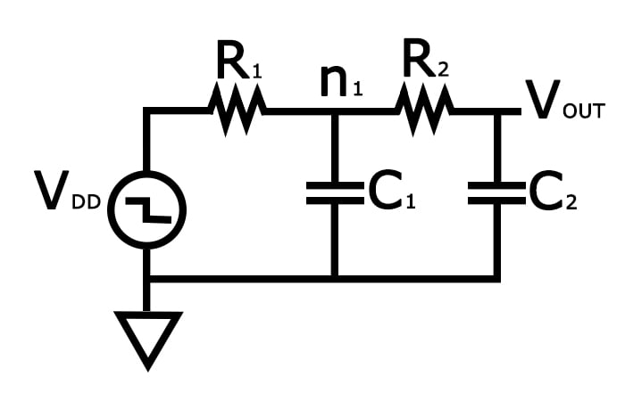
Figure 1
The Elmore delay for Vout is given as tpd = R1C1+(R1+ R2)C2 , which is similar to the delay expression gotten for the two-time constant (TTC) approximation model we discussed in the last article.
Let's consider a driver—i.e., a gate that charges or discharges a node or, in other words, a gate that is connected to the input of another gate. For our example, we'll look at a driver which is w-times the unit size which is driving an m-identical inverter. The equivalent RC circuit is shown in Figure 2.
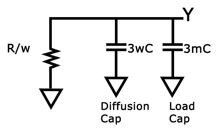
Figure 2
\[t_{pd}=(3w +3m)C\frac{R}{w}= (3+3\frac{m}{w})RC)\]
Equation 1
From equation 1, if we denote the fan-out of the drive to be the ratio between the load capacitance (3mc) and the input capacitance (3wc), we get the following:
\(h=\frac{3mc}{3wc}= \frac {m}{w}\)
Then, we can rewrite Equation 1 as
\(t_{pd}=(1+h)3RC\)
Equation 2
where τ=3RC.
Parasitic Delay and Logical Effort
Let's look back at the NAND gate given in the RC delay model article. If the NAND gate is set up to drive “h” identical NAND gates, that means it will see an additional “5hC” capacitance in the load capacitance value as shown in Figure 3.
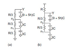
Figure 3. Image adapted from CMOS VLSI Design (4th ed.) by Neil H.E. Weste and David Money Harris
If we look at the worst-case scenario for the rise transition (as shown in Figure 3(b)), the PMOS transistor will pull the output node Y to HIGH while the active NMOS also contributes parasitic capacitance, which slows down this transition.
Note that the resistance “R” is charged along the path to the output node “Y”. The resistor of the two NMOS transistor circuit is not, however, considered since there is no output path across them. This is why they only contribute 6C capacitance value to the output node Y.
Given this, we get the following:
\[t_{pd}=R(9C+5hC+6C)\]
\[t_{pd}=R(15C+5hC)=(15+5h)RC\]
\[t_{pd}=(5+\frac{5}{3}h)RC\]
Equation 3
By observation, we can see that the delay has two components: the constant part and the one stated in terms of fan-out “h”.
The constant part is called the parasitic delay, which is the time for a gate to drive its internal capacitance (5C in this case). The parasitic delay for the inverter in equation 2 is 1.
The other part is the effort delay or electrical effort, which is the time to drive the load capacitance to the drive’s capacitance, this is also sometimes called logical effort. Similarly, the logical effort of the inverter in Equation 2 is 1 while the logical effort for the NAND in Equation 3 is \(\frac{5}{3}\).
Logical effort measures the worst a gate is at producing output current as compared to an inverter. This concept is crucial to analyzing the delay of any standard basic logic gate in combination with a load that can be abstracted as a logic gate module or a functional block.
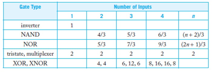
The table below shows the logical effort of common gates.
Table 1. Logical Effort of Common Gates
Variations of the Elmore Delay
The Elmore delay is extremely efficient to compute and it gives insight into the approximation algorithms discussed in the previous article. It has also been shown to have good fidelity when computed using a Hspice simulation. Further improvements have been proposed, such as the Fitted Elmore Delay1 and the Improved Elmore Delay2 models.
However, Elmore's delay can't accurately determine the logical effort of a gate, which is important in modeling large VLSI systems. To address this, we will need to discuss a new model to help determine how to keep the parasitic delay minimal without increasing the transistor size. So, in the next article, we'll be discussing “logical effort” for single and multiple paths.
References
- Arif, A.-S. I., Brian, N., & Chris, C. (2004, June 28). Fitted Elmore Delay: A Simple and Accurate Interconnect Delay Model. EEE Transactions on Very Large Scale Integration (VLSI) Systems, 691-696. doi:10.1109/TVLSI.2004.830932
- Mutlu, A., & Serhan, Y. (2010, April 8). An improved Elmore delay model for VLSI interconnects. Mathematical and Computer Modelling, 51(7), 908-914. doi:https://doi.org/10.1016/j.mcm.2009.08.024
Related Content