Facebook
 Google
 GitHub
 Linkedin
The Linear RC-Delay Model in VLSI Design
In this article, we'll discuss how a single transistor can be sized to properly integrate with other transistors to provide optimal performance in terms of speed and power.
As everyone is aware, a great deal of work has been put into making the transistor smaller. There is, however, still a need for corresponding work to go into VLSI circuits and modules in order to accommodate for smaller designs. These VLSI circuits and modules may be as simple as few logic gates (those which contain two to four transistors) or they may be larger systems that contain thousands and millions of transistors. Conversely, there is a need for these systems to meet speed/delay and power requirements in various working conditions.
In this article, we'll discuss how a single transistor can be sized to properly integrate with other transistors with these needs in mind. We'll do so by first covering the RC-delay model.
This article is part of a series in which we'll also discuss other popular models such as the Elmore delay and logical effort, which are used to estimate the delay of VLSI circuits. In these subsequent articles, we will also look at how these transistors and gates can be combined to provide an optimal area while also giving optimal performance.
The Linear RC-Delay
Like most electrical systems, transistors can be modeled as a simple RC circuit where the width of the channel is modeled as a resistor while the space between the diffusion (i.e., source/drain) is modeled as a capacitor.
This creates an RC network which is known for having an exponential rise/fall transient response whenever a step-input is applied at the input—in this case, the gate of the transistor. The rise/fall time (which is the time it takes for the output voltage level to match the input voltage level) defines the delay of a transistor circuit.
Calculating the Resistance of a Transistor
Now, what is an effective resistance of a transistor? How do we calculate the resistance of a transistor?
Typically, the resistance of a transistor is the ratio between the drain-source voltage and the drain-source current.
In modeling, a unit NMOS transistor has an effective resistance of R, which is equal to the resistance of the minimally-sized NMOS transistor used in the cell library or process. And because a transistor with a large width drives more current, an NMOS transistor of k-times unit width has a resistance of \(\frac {R}{k}\). And because PMOS transistors have lower mobility, its effective resistance is usually \(\frac{2R}{k}\).
The Effective Capacitance of a Transistor
The effective capacitance of a unit NMOS/PMOS transistor is “C” or “kC” for a k-times unit width. The equivalent RC circuit for an inverter driving a similar inverter is shown below in Figure 1.
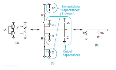
Figure 1. All images adapted from CMOS VLSI Design (4th ed.)1 by Neil H.E. Weste and David Money Harris
Since an inverter has a 2-times unit for PMOS transistor size and a unit width for NMOS, it usually offers a total of 3C input capacitance to the driving circuit.
As a recap, when the input is HIGH (3.3V), the NMOS (bottom transistor) is switched ON, and it gives resistance of “R” while pulling down the output voltage to ground (0V). But when input is LOW (0V), the PMOS (top) is switched ON, and it also gives resistance of R while pulling the output voltage to HIGH (3.3V).
This means, in a rise/fall transition, the effective resistance of the equivalent RC circuit is “R”. Meanwhile, the total capacitance of each transistor (3C) does not change with the transistor. Since we have two inverters cascaded together, they give a total of 6C capacitance.
Sizing a Transistor for a 3-Input NAND Gate
To further understand how transistors are sized in a logic gate, let's take a look at a 3-input NAND gate.
As a reference, a NAND gate will give a HIGH output if any input is LOW. Conversely, the output will be LOW when all the inputs are HIGH. This gives us three PMOS connected in parallel—only one PMOS is enough to pull the output voltage to HIGH—and three NMOS connected in series—the three NMOS need to be switched on before they can pull the output voltage to LOW.
To effectively size each transistor, we have to note that the transistor in the circuit has to be sized in a way such that the NMOS portion will give a unit resistance “R” and the PMOS portion must give twice the unit resistance of “2R” to ensure equal rise/fall time.
Since three NMOS transistors are connected in series, they must contribute a total resistance of \((\frac{R}{3} + \frac{R}{3} + \frac{R}{3} = R)\) where k = 3. Since only one PMOS is enough to pull the output to HIGH, in a worst-case scenario, each PMOS transistor maintains an effective resistance of \(\frac {2R}{2} = R \) where k = 2.
At a rise/fall transistor, each input will present an input capacitance of 5C while the total output capacitance output terminal Y is (2C+2C+2C+3C = 9C).
Moving forward, the equivalent RC circuit can be developed to give the circuit shown in Figure 2(c) and 2(d).
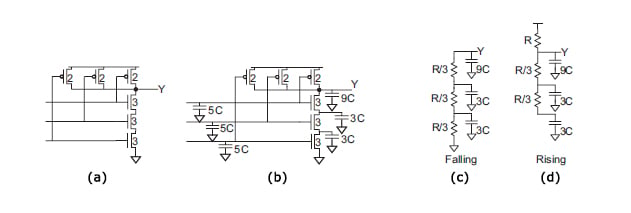
Figure 2.
The fall transition (2(c)) shows that all the NMOS transistors need to be switched ON while the rise transition (2(d)) shows a worst-case where one PMOS is switched ON while two NMOS transistors are ON, as well, contributing to the total capacitance of the circuit.
Assessing the Transient Response of the Circuit: Propagation Delay, STC, and TTC
After deriving a befitting equivalent RC circuit, the next step is to examine the transient response of the circuit. If we examine the equivalent RC circuit of an inverter shown in Figure 3 below, the goal is to estimate the time at which the input voltage will be seen at the output.
The time between when the input (VDD) is applied and when the output is \(\frac {V_{DD}}{2}\) is known as the propagation delay. The expression of the propagation delay can be derived from the classical transfer function of a first-order circuit given as:
\[H(s)=\frac{1}{1+sRC}\] and \[V_{out}=V_{DD}e^{-\frac{t}{RC}}\]
Therefore, the propagation delay is the time-constant (τ) of the transient response which is:
\[ t_{pd}=RC\]
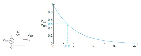
Figure 3.
From the delay response in Figure 3, the goal is to push the propagation delay close to zero to produce a faster circuit in general. In literature, this approach is popularly known as the single-time constant (STC) approach, which is a simplistic way of estimating circuit delay.
However, this approach seems inaccurate when estimating the delay of larger circuits, which led to the development of the two-time constant (TTC) approximation which gives us the luxury of having a better delay estimate due to the second time constant.
Examining the 3-input NAND gate discussed above, its RC circuit can be given as shown in Figure 4.
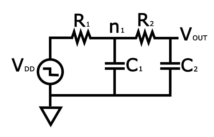
Figure 4.
And the step response of this circuit is given as
\[H(s)= \frac{1}{1+s[R_1C_1+(R_1+R_2)C_2]+s^2R_1C_1R_2C_2}\]
and
\[V_{out}(t)=V_{DD}\frac{\tau_1e^{ - \frac{\tau}{\tau_1}}-\tau_2e^{ - \frac{\tau}{\tau_2}}}{\tau_1 - \tau_2}\]
where
\[\tau_{1,2} = \frac{R_1C_1+(R_1+R_2)C_2}{2}\left [ 1\pm \sqrt{1-\frac{4R^*C^*}{[1+(1+R^*)C^*]^2}} \; \right ]\]
and
\[R^* = \frac{R_2}{R_1}; C^* = \frac{C_2}{C_1}\]
But due to the complicated nature of the TTC approximation, this defies the purpose of simplifying CMOS circuit delay into a simple RC network. However, it can be simplified by the STC model to give an approximate time constant (τ).
\[\tau=\tau_1 + \tau_1 = R_1C_1+(R_1+R_2)C_2\]
Single-Time Constant (STC) vs. Two-Time Constant (TTC)
According to Mark Alan Horowitz1, this approximation works best if a one-time constant is significantly larger than the other.
However, according to Neil H.E. Weste and David Money Harris2, this approximation is believed to give an error of 7%-15% and therefore does not give an accurate delay description of intermediate nodes.
Additionally, the RC delay model usually results in larger integration/differential equations which are usually time-consuming to solve and/or simulate in larger systems. This has led to the development of a better STC approach which was proposed by Elmore. It is called Elmore Delay Model which will be discussed in detail in the next article.
References
- Horowitz, M. A. (1984). Timing Models for MOS Circuits. Stanford University, California.
- Weste, Neil H.E. & Harris, David Money (2011). CMOS VLSI Design (4th ed.). Boston: Addison-Wesley.
Related Content