 Facebook
 Google
 GitHub
 Linkedin
How to Buffer an Op-Amp Output for Higher Current, Part 3
The previous two articles focused on bipolar junction transistors. In this article, we’ll look at buffering with MOSFETs instead of BJTs.
The previous two articles focused on bipolar junction transistors. In this article, we’ll look at buffering with MOSFETs instead of BJTs.
Supporting Information
- Introduction to Operational Amplifiers
- Class B Audio Amplifier
- Insulated-gate Field-effect Transistors (MOSFET)
Previous Articles in This Series
- How to Buffer an Op-Amp Output for Higher Current, Part 1
- How to Buffer an Op-Amp Output for Higher Current, Part 2
BJT vs. MOSFET: The Ongoing Rivalry
I often wish that there were a concise, definitive answer to the old question, “Which are better, BJTs or MOSFETs?” But as you probably know, this is like asking, “Which are better, cars or trucks?” With both questions, there is no universal answer; rather, the details of each situation determine which option is preferable. In this article we will explore the use of MOSFETs in the specific context of buffering an op-amp output for higher current, and in the process we will be able to form a general idea of when MOSFETs might be preferable to BJTs, and vice versa.
A Brief Review
First let’s review some salient MOSFET characteristics.
- The current flowing through the MOSFET’s channel is controlled almost entirely by the gate-to-source voltage when the FET is operating in the active (aka saturation) region; in the linear (aka triode) region, current depends also on the drain-to-source voltage.
- The MOSFET begins to conduct current when the gate-to-source voltage exceeds the threshold voltage. The amount of current (in the active region) is proportional to the square of the overdrive voltage, which is defined as the gate-to-source voltage minus the threshold voltage.
- The gate of a MOSFET is insulated from the rest of the device, such that the steady-state current flowing into the gate is almost zero. I say “almost zero” because some leakage current flows through the gate dielectric; for our purposes this leakage current is negligible, though it is a problem with the extremely thin (i.e., less than 2 nm) gate dielectrics used in modern integrated circuits.
- The physical structure of the MOSFET’s gate results in a relatively large capacitance—in the context of this article’s subject matter, maybe as much as 5 times higher than the input capacitance of an equivalent BJT.
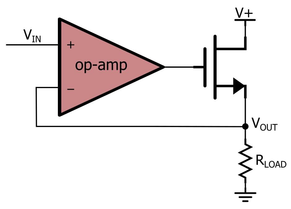
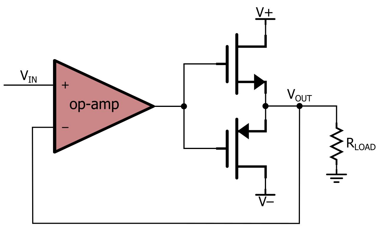
NPN Out, NMOS In
Here is the first buffering configuration with a MOSFET instead of a BJT:
And here is an LTspice circuit:
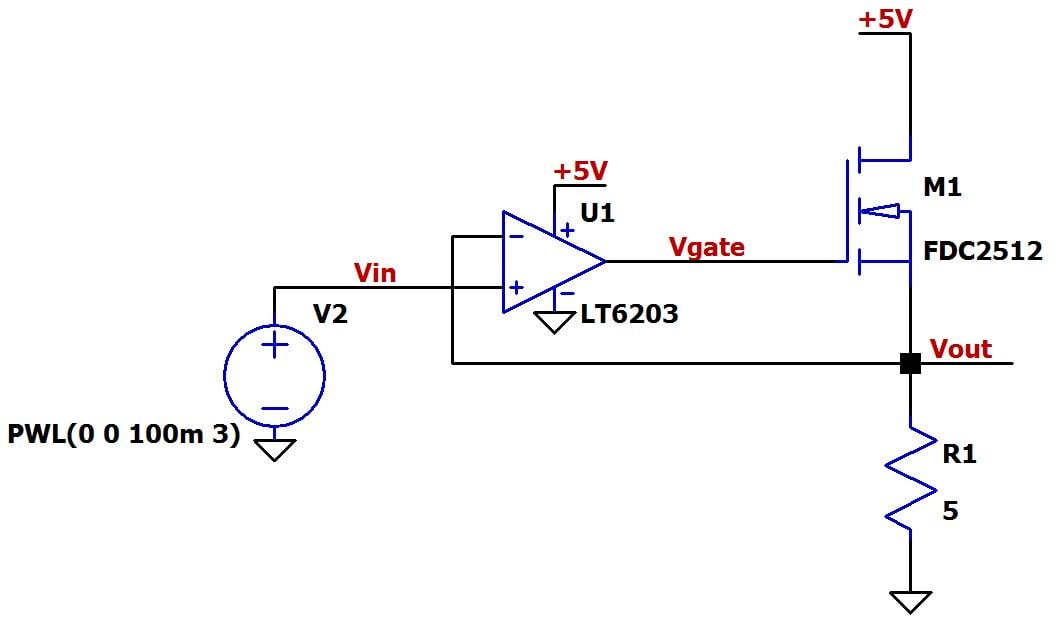
I chose the NMOS part based on maximum drain current; I wanted something similar in capability to the 2SCR293P NPN used in Part 1, so that the comparison is more meaningful. The 2SCR293P’s maximum continuous collector current is 1 A, and the maximum continuous drain current for the FDC2512 is 1.4 A. The two parts also have similar power dissipation limits. As expected, there is a significant difference in input capacitance: for the 2SCR293P, about 90 pF; for the FDC2512, about 375 pF.
Threshold Voltage
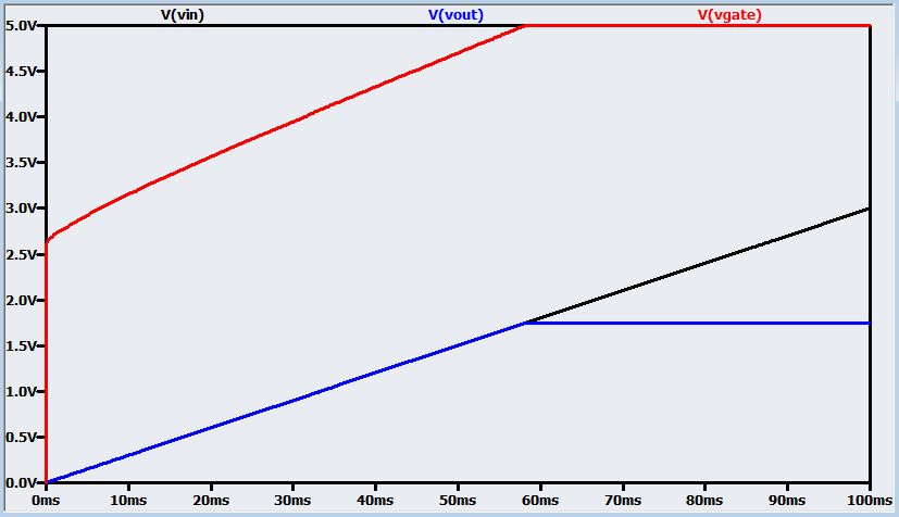
Here is a plot with VIN and VOUT.
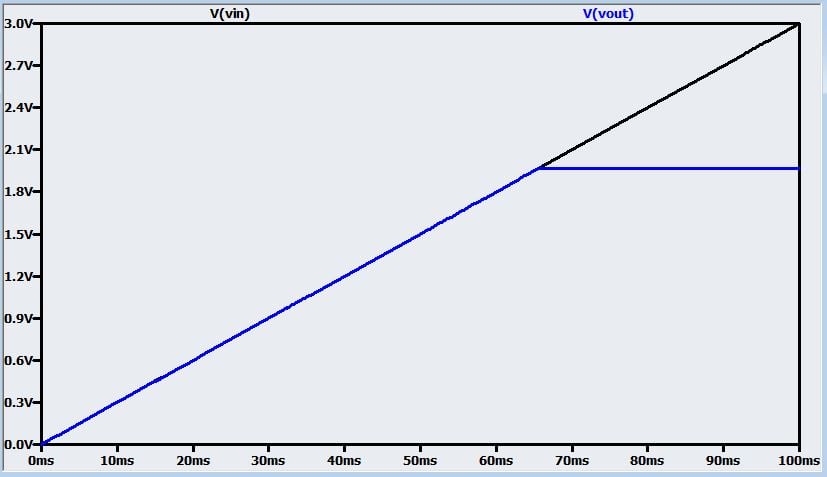
A problem is immediately apparent: the load voltage levels out at just below 2 V, even though we have 5 V supplies for the NMOS and the op-amp. The next plot reveals the cause.
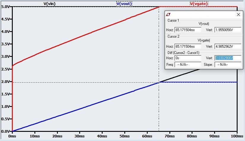
As you can see, the gate voltage saturates at the op-amp’s positive supply voltage when the load voltage is only about 2 V. The main problem here is the MOSFET’s threshold voltage: the FET doesn’t even begin to conduct until the gate-to-source voltage is 2.6 V. This means that the op-amp’s output voltage will always be at least 2.6 V higher than the load voltage, because the voltage difference will only increase as more drain current is required—as shown in the previous plot, the gate-to-source voltage is 3 V when the output levels off. Actually, the voltages shown in the plot represent the typical characteristics of the FDC2512; according to the datasheet, the threshold voltage could be as high as 4 V!
This first simulation demonstrates a major disadvantage of using an NMOS transistor in this circuit: the threshold voltage is much higher than the 0.7–0.9 V required for an NPN’s base-emitter junction. Of course, threshold voltage varies from part to part, so you could certainly mitigate this problem by choosing a different FET. A quick Digi-Key search indicates that NMOS transistors rated for 1–2 A continuous drain current can have threshold voltage much lower than 2.6 V. Nevertheless, you need to be careful here, because NMOS threshold voltage tends to be higher than the 0.7–0.9 V base-to-emitter voltage you can expect from just about any NPN transistor. Even a Darlington pair (discussed in Part 2) will provide load voltage range similar to or better than what you would get from some MOSFETs, and the Darlington reduces base current to levels that just about any op-amp can handle.
Another detail to keep in mind is the following: the load voltage range becomes more limited with larger load currents because the op-amp must create a higher overdrive voltage to produce the higher drain current. If we set the load resistor to 2 Ω instead of 5 Ω, we get the following plot:
In this case the load voltage levels out at about 1.75 V instead of 2 V.
Sinking and Sourcing
This discussion about the NMOS transistor is relevant also to a PMOS transistor that you would use as the current-sinking device in a Class B output stage (discussed in Part 2).
The performance of an NMOS–PMOS stage would be comparable to that of an NPN–PNP stage; just make sure you choose your FETs carefully for adequately low threshold voltage.
Here is an LTspice schematic:
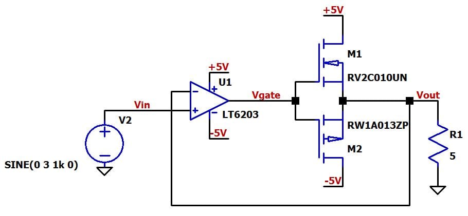
I was having trouble finding suitable parts among LTspice’s built-in NMOS and PMOS options, so instead I’m using two low-threshold-voltage FET models from ROHM Semiconductor. The NMOS is part number RV2C010UN, and the PMOS is part number RW1A013ZP. The links attached to these part numbers will take you to product pages where you can download the SPICE model (on the right under “TECHNICAL DATA”), and you can go here for an explanation of how to use a third-party model with the LTspice NMOS and PMOS components.
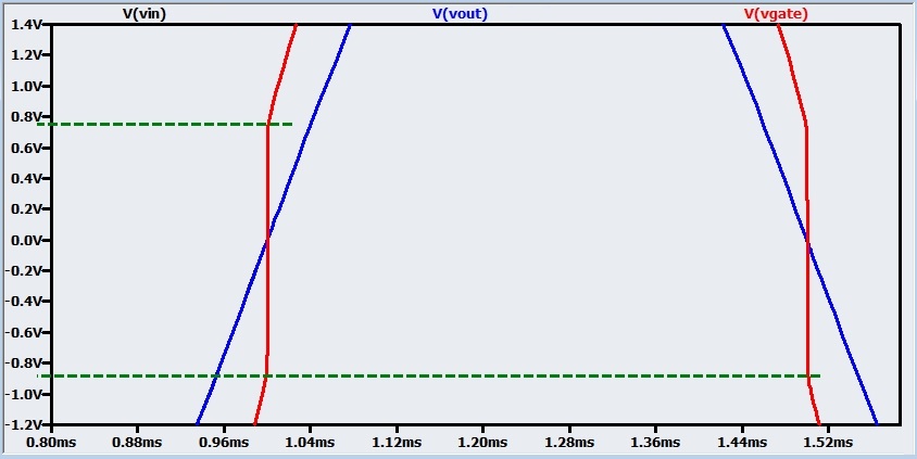
Here is a plot with VIN, VOUT, and VGATE:
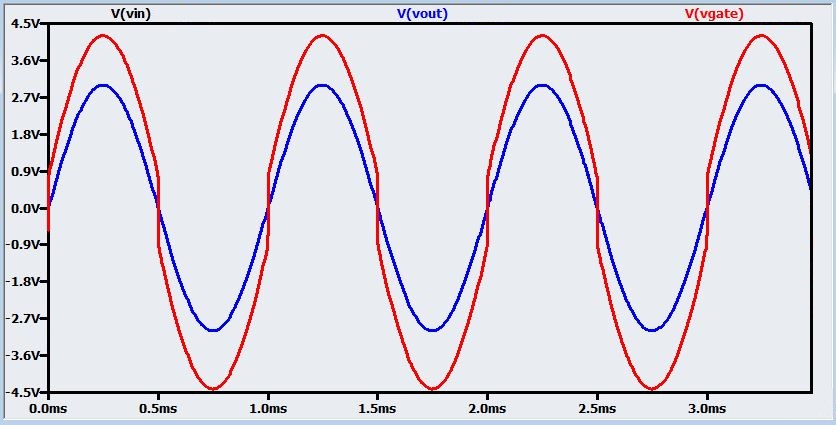
VIN is hidden under VOUT. As with the BJT version, the op-amp’s output voltage (i.e., VGATE) bypasses the dead band in which both FETs are in cutoff. Also, this plot is great for visualizing how the difference between VGATE and VOUT increases as VOUT (and therefore also the load current) increases; this reflects the fundamental active-mode operation of a MOSFET, namely, higher drain current requires more overdrive voltage.
If we zoom in, we can see that the threshold voltage for the NMOS and the PMOS is about 0.75 V and 0.9 V, respectively. So with these particular parts, the threshold voltage is not much higher than a BJT base-to-emitter voltage drop.
Conclusion
The basic op-amp current buffering circuits can work well with both BJTs and MOSFETs. The primary benefit of the MOSFET is the negligible output current required from the op-amp, and the primary concern is that the output voltage range can be restricted by relatively high gate-to-source voltages. In the next article we will explore a subtle but significant issue that can complicate the use of MOSFETs for op-amp current buffering: the effect of gate capacitance on stability.
Next Article in Series: How to Buffer an Op-Amp Output for Higher Current, Part 4


Sir if the load changes that mean if R(load) changes then the current through it also changes significantly.
Sir how can we make this circuit load resistance independent.