 Facebook
 Google
 GitHub
 Linkedin
Schematic Design for a Solar-Powered Charge-Pump Power Supply Circuit
This article discusses a 3.3 V power-supply circuit that is built around an inductorless DC/DC converter and a solar cell.
This article discusses a 3.3 V power-supply circuit that is built around an inductorless DC/DC converter and a solar cell.
Related Information
- Boosting and Inverting without Inductors: Charge-Pump Power Supplies
- The Circuit Designer’s Guide to Photovoltaic Cells for Solar-Powered Devices
- Selecting and Implementing Photovoltaic Cells for Solar-Powered Devices
I recently designed a circuit board that gives me an opportunity to explore the use of solar power for embedded devices. My idea was the following: I wanted a reference design that would serve as a very compact, very straightforward way of using ambient light to generate 3.3 V for a microcontroller-based embedded system. I’ve tested the board enough to confirm that it does work, though it also has major limitations. In this article I’ll focus on the schematic design for the board.
Keeping It Small
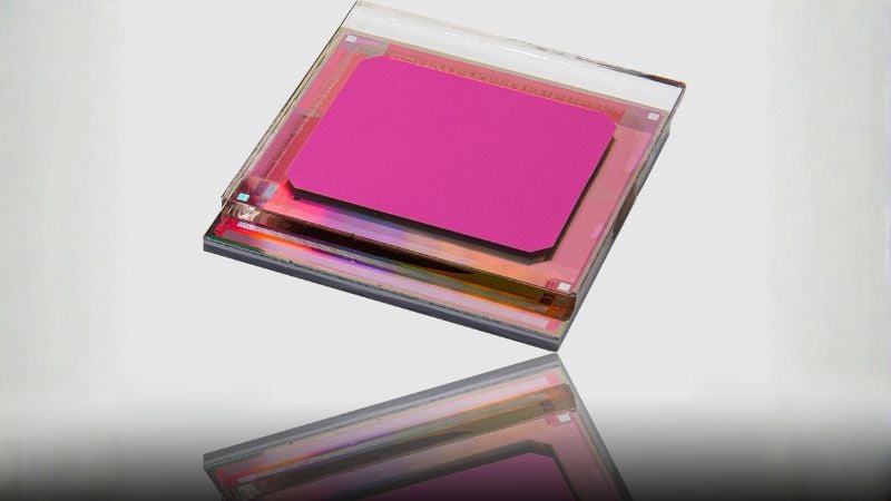
My general goal with this project was to develop a simple way to incorporate solar power into small, low-power devices such as wearables and IoT sensors. I’m not too impressed with the performance that I’ve observed so far, but the size of the overall solution is pretty good. The primary components are a 7 mm × 22 mm monocrystalline solar cell (p/n KXOB22-01X8F) and a tiny charge-pump DC/DC converter (p/n LTC3204EDC-3.3).

Image taken from this datasheet.

Image courtesy of Digi-Key.
All you need in addition to the solar cell and the charge pump is capacitance: an input capacitor, a capacitor for the charge-pump circuitry, and an output capacitor. It’s good to know that you can convert sunlight into a regulated 3.3 V supply with only one solar cell, one miniscule six-pin IC, and three capacitors. What’s even better is that all three capacitors can be the same value; this makes ordering the parts and assembling the board a little bit simpler.
My Implementation
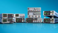
The following schematic excerpt shows my design for a solar-powered 3.3 V power supply. I included four output capacitors; this enables me to add and remove caps as a way to experiment with the effects of higher or lower output capacitance. As mentioned above, though, only one output capacitor (minimum 2 µF) is required.

As you can see, it’s difficult to compete with the simplicity of this approach. The BOM has three line items, and the interconnections are very straightforward. All the capacitors can be surface-mount ceramic types; I recommend X7R. The hardest part is installing the LTC3204, which is not only tiny but also a no-leads package with a thermal pad. With the help of my hot-air gun and some low-temperature bismuth-based solder paste, I was able to get it done without too much difficulty.
Limitations
Before I say any other positive things about this design, let’s review the negatives:
- It doesn’t have a supercapacitor or a battery; in other words, it has no means of long-term energy storage. This is a “works when the sun is shining” device.
- The charge-pump IC achieves proper regulation only when the solar cell is exposed to full sun. This was an unexpected limitation that I’ll explore further in the upcoming project article. The bottom line, as far as I can tell, is that only full sun generates enough solar-cell current to adequately supply the input current required by the LTC3204.
- Even under full-sun conditions, the available output current is quite low. The solar cell maxes out at 4.4 mA, which isn’t really enough for high-speed microcontroller operation, and my guess is that RF communication wouldn’t be too feasible either.
The MCU
My board includes not just the solar-powered charge-pump supply but also a microcontroller circuit:
Click to enlarge.
- The microcontroller is an EFM8 Sleepy Bee from Silicon Labs. It requires only 90 µA of supply current when running at 32.768 kHz.
- A switch allows me to power the microcontroller from the solar-cell circuit or from the Silicon Labs USB debug adapter. The debug adapter provides 5 V, so you need an LDO (the Sleepy Bee’s VDD range is 1.8–3.6 V).
- The 32.768 kHz crystal allows me to achieve both low current consumption and high precision for real-time clock applications. No capacitors are required; you connect the crystal directly to the XTAL3 and XTAL4 pins and then configure the load capacitance via firmware.
The Charge Pump
The LTC3204 comes in four flavors: the (fixed) output voltage can be either 3.3 V or 5 V, and the part can operate in either burst mode or constant-frequency mode (there’s no “mode select” pin; you have to specify the part number that corresponds to the desired mode). I opted for burst mode. I’m not sure if this offers significant benefits in the context of solar power, but the “no-load input current” is much lower in burst mode, and this seemed like a beneficial feature considering my solar panel’s output-current limitations.

Taken from the LTC3204 datasheet. The part numbers with the “B” suffix are, rather confusingly, the non-burst-mode versions.
The LTC3204 maintains a regulated 3.3 V output with input voltages from 1.8 V to 4.5 V; this makes it a fairly good match for the KXOB22-01X8F solar cell:

Plot taken from this datasheet.
The solar-cell voltage can go as high as 4.7 V, which strictly speaking is beyond the LTC3204’s input range. However, the absolute maximum input voltage is 6 V, so the solar-cell voltage will never exceed or even approach the absolute max, and I doubt that a 4.7 V input will cause any problems.
Conclusion
We’ve looked at the schematic design for a solar-powered microcontroller board that uses a simple, compact charge-pump IC to generate a regulated 3.3 V power rail. It’s a small and fairly inexpensive solution that could be incorporated into various low-power devices. It has significant limitations, though, and I currently have plans for a modified design that requires more PCB real estate but in exchange offers higher performance and easier assembly.
Related Content


I should think you need MPTT a to get anywhere with that small solar cell. Is there a reason for not going this route?
Note that the output specification for your solar cell is _no_load_. Once you have a load on it (such as the charge pump), it will not be able to achieve the 4.7V output anyway. You should be able to measure the no-load voltage in full sun, then the voltage with the charge pump (but not uC) connected, and finally, with the uC also connected.