 Facebook
 Google
 GitHub
 Linkedin
Special Topics in Schematic Capture
Learn about heterogeneous and homogenous buses, special IC packages, and more!
Learn about heterogeneous and homogenous buses, special IC packages, and more!
This article is a collection of special topics about the creation of schematic diagrams. The topics are ones I have carried around in my head for years. I hope you find them useful.
This article assumes experience with building schematic symbols and creating basic schematics.
High Pin Count Parts
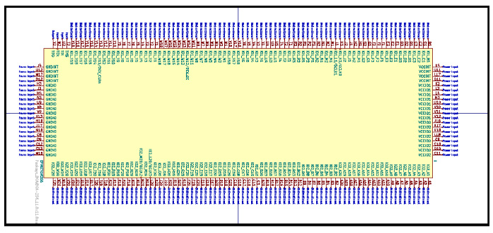
Here is the highest pin count symbol I found from a quick search of KiCAD libraries. To me, this is too dense and totally impractical. There should be a rule against this sort of thing! I went back over a bunch of my schematics and found my threshold is around 100 pins. Over 100 pins and I always created multiple units per part.
I break up a high pin count part by splitting the pins into functional groups. For example, an FPGA will have one unit for all the power and ground pins. Another unit will have all the pins associated with configuring the part. Then, there are multiple units for the I/O pins.
Here is a unit for the configuration pins of an FPGA.

This symbol can be placed anywhere in the schematic that makes sense. In this case, it is with the configuration memory IC and the JTAG connector used for programming and debugging. Also on the sheet are several miscellaneous things which needed a home.
Here is the unit with the power and ground pins.

There is not much structure to the power pins. Two types of power pins are in two groups: internal power in one group and I/O power in another group. Other devices have much more complex power structures and would need more groups. This unit is on a sheet with voltage regulators and power-monitoring circuits.
The I/O pins are split into four units. Here is one unit showing about 25% of the I/Os.

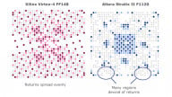
Altera (now Intel) parts often have internal interconnects with a prominent row and column structure. In this part, the I/O speed is faster for I/Os connected to row interconnects and slower for I/Os connected to the columns. Since this was a high-speed design, I needed to consider which signals were connected to rows or columns, and I created a symbol that helped me in the pin assignment. You can see that this unit is all “row” pins. In addition, the rows are further grouped together (ROW A, B, C, etc.). This arrangement indicates other timing characteristics inside the device.
Consider grouping I/Os in programmable devices to reflect the functionality of the part in a particular design. The extra work for custom symbols is OK with me if it helps in the design and understanding of the circuit.
Hierarchy
In general, schematics larger than one sheet can be organized in two ways, flat or using hierarchy. Flat schematics use connections directly from sheet to sheet. A signal typically goes off the side of one sheet and appears on the side of another sheet. Hierarchy uses a “hierarchical block” in a sheet to represent another sheet. Connections to the sheet are done by connecting to the block. There can be multiple hierarchical blocks on a sheet. The organization of blocks and sheets can look a lot like a file directory in a computer. There is usually a “root sheet” which is a lot like a root directory.
Hierarchy is used for two main purposes. First, it provides for a logical structure within the schematic and a way to navigate between sheets in a way that is consistent with signal connections. Second, it allows circuitry to be drawn once on a sheet but repeated multiple times by using multiple hierarchical blocks that reference the same sheet.
Using hierarchy is a powerful way to organize a design. It takes a bit of work to get comfortable with this sort of structure. However, for me, it has become essential. I use it so much that I never have the direct sheet-to-sheet connections used in a flat design. A sheet is always connected through a hierarchical block. The subtle effect is the schematic takes on the appearance of a three-dimensional block diagram. I like the way this documents the design and makes it quick and easy to find things.
Here is the root sheet of a 20-channel high-voltage amplifier board. Of course, it is not possible to see detail. However, perhaps you can see how the hierarchical blocks look like a block diagram.

I provide notes to list what circuitry is in each block. Clicking into a block makes it easy to find something. Not here but in other designs, I included blocks on the root sheet with no circuit connections but referencing sheets with notes and diagrams. Using blocks like this works like a table of contents with links.
I notice an I2C bus in the middle with three signals: I2CSDA, I2CSCL, and I2CINT. I wish I had been able to use a “heterogeneous bus” which is the next topic! I could have condensed three lines into one!
Homogeneous and Heterogeneous Buses
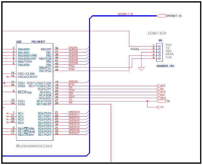
All the schematic programs I know support collecting multiple, similarly named nets into a “bus”. The term originally came from bundling signals in a data bus or address bus. In the schematic below, this feature bundles signals with the name “SHDN” followed by sequential numbers. This is called a “homogeneous” bus.
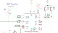
In the middle of the schematic is an SPI interface with four signals: SS, SCK, SDI, and SDO. They are a functional group, and it would be handy to combine them and use one line and one name for all of them. Some schematic programs allow signals to be grouped into a “heterogeneous” bus. There doesn’t seem to be a standardized name for this type of bus. Altium calls it a “Signal Harness”. OrCAD uses the term “NetGroup”. In Eagle all buses are heterogeneous. KiCad is developing this feature and calling it a “Group Bus”.
Here is a heterogeneous bus created in Eagle for the four nets in the schematic.

In my opinion, a heterogeneous bus provides logical structure to the schematic and reduces clutter.
Special IC Packages
Mechanical designers have become quite clever in solving packaging issues related to smaller and smaller form factors and thermal management. However, some of their designs cause connections that should be shown on a schematic. I try to include in the schematic any package element that connects to a net. For example, a plated-through mounting hole for a connector shell or a thermal tab on a part that connects to GND or power should be in the schematic. Here are two examples of packages with features connecting to power or GND.

The part on the left has a metallic tab that is usually soldered to a copper area on the top of the board to dissipate heat. The part on the right has an “exposed pad” on the bottom that is soldered to a copper area. In both cases, the tab or pad is often electrically connected inside the IC.
This schematic shows how I handled the exposed pad for a voltage regulator using the package on the right.

Pins 1 to 5 are the normal pins. I added Pin 6 to represent the electrical connection to the exposed pad and connected it to GND. I also included 6 thermal vias that conduct heat from the top to the bottom copper areas. The vias are included in the schematic because they make an electrical connection. Here is the result:

Question: When is a 64-pin part not a 64-pin part?
Answer: When it is an “E64” package.
When building a symbol for this part you immediately see there are no ground pins on the part! One commenter in an Intel forum speculated it was a cutting-edge part using a quantum effect and no ground connection was needed. Well, not quite. Ground is an exposed pad on the bottom of the part. Here is the drawing of the bottom with the pad in the middle.

To deal with a part like this, just add a Pin 65 to the symbol. Then, connect it to GND in the schematic. Be sure to add a note on the schematic! The datasheet points out that the pad is only for electrical connection and has no thermal function. The PCB designer will need to know that!
Bonus Topic
“Back in the old days” schematic diagrams were hand drawn, most often by a professional draftsman. From time to time, they might take a break and doodle on the schematic about something that sparked their imagination. Here is an example from a Tektronix schematic.

Image used courtesy of vintageTEK
-
Have you ever added a cartoon or emoji to a schematic?
-
Have you ever used a non-orthogonal line for a net? Does your schematic program allow them?


If I remember correctly Ford Motor Co. calls their heterogeneous bus lines multiplex?
YES! Thank you. My most recent complex design uses an EP3SL200F1517… it has 1517 pins. This would be far, FAR beyond impossible to include in a coherent schematic the way too many schematics are drawn these days. Instead, I broke it down much as you did. Core power, config, communications, and each I/O bank in a separate module. Each I/O banks supply power is included at the top of its respective block so that seeing what voltage each bank is running at is trivial.
The “schematic” supplied with the evaluation board has one huge rectangle, with 1517 pins along its perimeter, each going out to a label. On some other page, you can find this label and eventually find what it connects to. Then after consulting the pin description, and going back to the original page, you can eventually find what voltage that I/O bank is running at. “Schematics” like this drive me crazy. Come on people, have some pride in your work.
Let me say here that the purpose of the SCHEMATIC is to *schematically* explain to the user the functioning of the circuit. A handy additional function of computer generated schematics is that their output can also be handed directly to a layout program and populate a “ratnest” of the desired connections. The way many “schematics” are composed these days is nothing more than a graphical net-list, that could be just as well presented as a text file, with IC#, Pin# and signal name all in a linear list, and the router could figure it out. That would satisfy the routing program but would give almost ZERO information to the user about the functioning of the circuit. NOT the purpose of a proper schematic.
A classic example is the quad (or more) amplifier or logic-gate. It is not a 14/16-pin rectangle, it is 4 separate items with a common power supply. To properly display it on a schematic, you use the schematic symbol of the amplifier (the triangle) or logic-gate (or/and/not/etc). Each one has a label like IC1a, IC1b, IC1c, etc. Seeing a rectangle with a bunch of wires haphazardly connected around the perimeter is NOT a schematic.
On my schematics, things like switching power supplies are also not just rectangles. The interior of the box has a sketch of the block-diagram from the manual. Multi-channel ADCs show the S/H, digitizer, output sequencer, mode selection, reference generation, etc. When looking at my schematics, the number of times you need to look at the manual to figure out what a chip is doing is reduce to *almost never*. THAT is the purpose of a schematic. What you are describing here goes a long way toward that end, and should be seriously considered by anyone who wants to generate a useful schematic.
Other things that can be of use are paralleling identically labeled pins. You don’t really need to show 137 ground pins on a single chip on the schematic. The library can connect them, the routing program will include all of them, but the *schematic* gains absolutely ZERO additional information with this multitude of identical purposed pins. It’s a schematic, not a wiring diagram. The wiring diagram is on the routing page. See how that works? Other things you don’t need on the schematic page is the package type, the orientation of the package, whether or not the item is on the top or bottom layer, etc. They too, go on the routing page.
There are multiple other layers of things that can be to create more understandable schematics, but not putting all the chips in blank rectangular boxes on the schematic page is probably at the very top of the list. Keep good information like this coming.