 Facebook
 Google
 GitHub
 Linkedin
The Basics of Emitter-Coupled Logic
This article will review the operation of a basic ECL inverter/buffer, and then we’ll look at some of the most important features of this logic family.
This article will review the operation of a basic ECL inverter/buffer, and then we’ll look at some of the most important features of this logic family.
Emitter-coupled logic (ECL) is a BJT-based logic family which is generally considered as the fastest logic available. ECL achieves its high-speed operation by employing a relatively small voltage swing and preventing the transistors from entering the saturation region. In the late 1960s, when the standard TTL family offered 20 ns gate delay and the CMOS 4000 family had delays of 100 ns or more, ECL offered an incredible delay of only 1 ns!
This article will review the operation of a basic ECL inverter/buffer, and then we’ll look at some of the most important features of this logic family.
Emitter-Coupled Logic
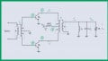
Emitter-coupled logic is a high-speed bipolar logic family. To get familiar with this logic, let’s examine an ECL inverter/buffer as shown in Figure 1. In this figure, $$V_{in}$$ is the input of the gate, $$V_{out-}$$ is the inverted version of $$V_{in}$$ and $$V_{out+}$$ is the complement of $$V_{out-}$$. In this particular example, $$V_{out+}$$ can be considered as the buffered version of the input. Moreover, $$V_{BB}$$ is an appropriate voltage (4V in Figure 1). Let’s define the logic high and logic low as 4.4 V and 3.6 V, respectively, and examine the operation of the circuit in Figure 1.
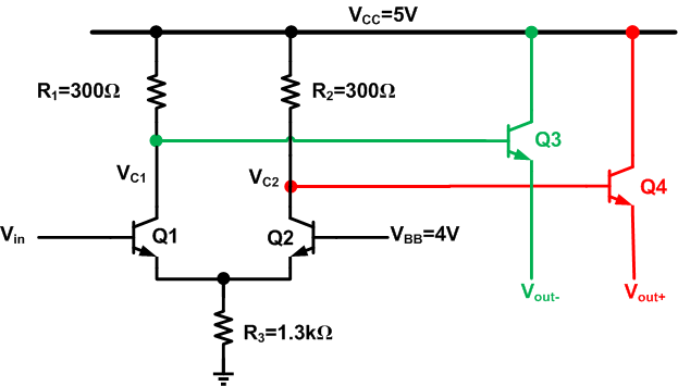
Figure 1. An ECL inverter/buffer
Assume that $$V_{in}$$ is logic high (4.4 V), hence the emitter of Q1 will be about 4.4-0.6=3.8 V. Therefore, the base-emitter voltage of Q2 will be 0.2 V. This base-emitter voltage is not sufficient to turn Q2 on. Hence, the resistor R2 will pull the collector of Q2 up to Vcc=5 V.
To calculate the collector voltage $$V_{c1}$$, we should note that the current flowing through R3, which is $$\tfrac{3.8V}{1.3k \Omega}=2.92mA$$, will go through Q1. Hence, we obtain $$V_{c1} = 5V-300 \Omega \times 2.92mA=4.12V$$ (to simplify the calculations, we’ve assumed that the collector current is equal to the emitter current). The emitter followers Q3 and Q4 will act as buffers to pass the (DC level shifted) collector voltages of Q1 and Q2 to the final outputs of the ECL gate, $$V_{out-}$$ and $$V_{out+}$$. Assuming a base-emitter voltage of 0.6V for Q3 and Q4, we obtain $$V_{out+}$$=4.4V and $$V_{out-}$$=3.52V. As you can see, applying logic high to the input gives a logic high at $$V_{out+}$$ and a voltage level very close to the defined logic low (3.6 V) at $$V_{out-}$$. Hence, the circuit of Figure 1 serves as an inverter/buffer.
If we apply the logic-low voltage (3.6V) to the input of the gate, Q2 will turn on and Q1 will be off. This will lead to a logic high at $$V_{out-}$$ and a voltage level very close to the logic low (3.61 V) at $$V_{out+}$$.
Now that you’re familiar with the ECL inverter/buffer, you should be able to verify that the circuit of Figure 2 implements an OR function of a and b or a NOR function of a and b, depending on how the positive and negative outputs are used.
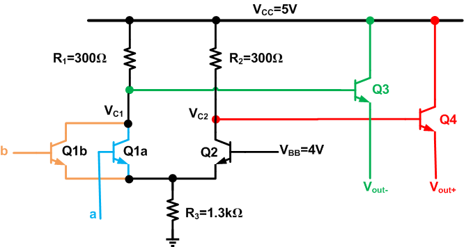
Figure 2
Low Voltage Swing
As you can see, the voltage difference between logic high and low of an ECL gate is much less than that of a CMOS or a TTL logic gate. This low voltage difference reduces the time required to make a transition from logic high to logic low or vice versa. As a result, ECL logic offers higher-frequency operation.
Avoiding Saturation
In addition to the low voltage difference between the logic levels, there’s another mechanism that significantly contributes to the high speed operation of an ECL gate. The trick is to prevent bipolar transistors from entering the saturation region. Turning off a saturated bipolar transistor requires removing or recombining some carriers generated in the transistor base region.
If we apply a high to low transition to the input of a saturated BJT, the transistor output won’t change until the charge in the base is removed. This introduces an extra delay, called storage time, to the operation of a BJT employed as a switch. After the storage time, the transistor comes out of saturation and the output of the transistor starts to respond to the input.
If appropriate resistor values are chosen, ECL logic prevents transistors from entering saturation. For example, in Figure 1, R1, R2, and R3 are chosen such that the collector voltage of Q1 and Q2 cannot be less than about 4.1 V. Based on the above discussion, the maximum emitter voltage of Q1 and Q2 is about 3.8 V. Hence, the collector-emitter voltage of these two transistors is always more than $$V_{C(min)}-V_{E(max)}$$=4.1 V-3.8 V=0.3 V. This is larger than the collector-emitter saturation voltage which is about 0.2 V. Therefore, Q1 and Q2 cannot enter the saturation region.
As discussed above, ECL avoids the storage-time problem by properly choosing the resistor values. Since the storage time can account for a significant portion of the propagation delay in other logic families, there are several other methods to reduce this undesired effect.
Positive-Referenced ECL
It’s worth mentioning that old ECL families used a negative supply voltage, as shown in Figure 3. That’s why an ECL gate such as Figure 1, which uses a positive supply voltage, is referred to as positive-referenced ECL or PECL (pronounced “peckle”).
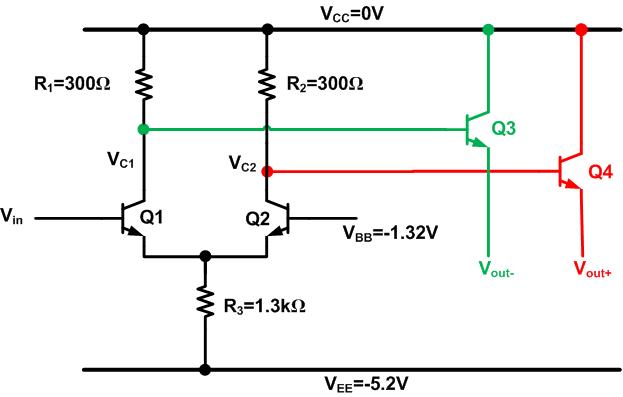
Figure 3
Noise immunity was the main reason for using a negative power supply with the early ECL gates. As the analysis of the ECL inverter/buffer shows, the output voltages of an ECL gate depend on the value of $$V_{CC}$$. For example, the logic high is equal to $$V_{CC}-V_{BE}$$, where $$V_{BE}$$ is the base-emitter voltage drop of the emitter followers. The logic low is $$V_{CC}-V_{BE}-V_{gate}$$, where $$V_{gate}$$ is the voltage difference between logic high and low, which is determined by the value of the resistors. Therefore, any noise on $$V_{CC}$$ will directly affect the ECL gate’s output voltages.
It is generally easier to achieve a stable, low-noise ground node than a stable, low-noise power-supply voltage. The early ECL families used a negative supply, and ground was used as the reference for the gate’s output voltages; this led to better noise immunity. However, PECL became popular because it interfaces more easily to other logic families such as TTL.
If a negative power supply is used, a clean ground needs to be distributed throughout the ECL-based portion of the design. The same considerations should be applied to power supply distribution when using positive-referenced ECL. For example, if both TTL and ECL are used in the system, it is recommended to use separate power planes for the two logic families so that the TTL switching transients don’t affect ECL operation.
Power Dissipation
In Figure 1, we saw that changing the logic state of the input makes the current flow through either Q1 or Q2. However, it should be noted that the total current flowing through Q1 and Q2 is almost the same for a logic-high input as it is for a logic-low input. As a result, the power dissipation of the first stage of the ECL circuit is almost constant.
During voltage transitions, CMOS logic gates cause transient disturbances in the power-supply voltage. A major advantage of ECL is that the current-steering behavior of the input stage (i.e., Q1 and Q2) does not cause disturbances in the way that CMOS switching does.
However, this noise performance is achieved at the cost of burning more static power. Note that a CMOS gate consumes power only during voltage transitions, whereas the differential pair formed by Q1 and Q2 (see Figure 1) almost always draws about $$\tfrac{4V}{1.3k \Omega} \approx 3mA$$ from $$V_{CC}$$.
If we focus on static power consumption, ECL is a high-power logic family. However, if we consider dynamic power consumption, ECL can be more efficient than CMOS, especially as the frequency of operation increases. This is shown in Figure 4.
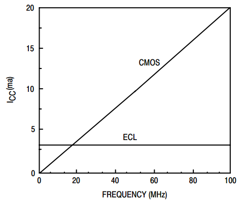
Figure 4. Image courtesy of ON Semiconductor.
Below 20 MHz, ECL draws more supply current than CMOS, but as we go beyond this frequency, ECL becomes more efficient. This is why ECL is an attractive solution for high-frequency clock distribution.
As a final note, the emitter followers (see Figure 1) must provide large output currents to charge load capacitances, and consequently they can cause significant transient deviations in the supply voltage. Thus, in some cases it is advisable to use two separate power supply lines: one for the input stage and one for the emitter followers. This can prevent the power-supply disturbances generated by the emitter followers from contaminating the ECL differential pair.
Summary
ECL is considered to be a very high-speed logic family. It achieves its high-speed operation by employing a relatively small voltage swing and preventing the transistors from entering the saturation region.
An ECL implementation that uses a positive supply voltage is referred to as positive-referenced ECL or PECL. Noise immunity was the main reason for using a negative supply voltage with the early ECL gates. Later, PECL became popular because its logic levels are more compatible with those of other logic families such as TTL.
ECL dissipates a relatively large amount of static power, but its overall current consumption is lower than that of CMOS at high frequencies. Thus, ECL is particularly advantageous in clock-distribution circuits and other high-frequency applications.
To see a complete list of my articles, please visit this page.


LS-APD-ECL is faster and consumes less power
CECL stands for Cascode Emitter Coubled Logic