Facebook
 Google
 GitHub
 Linkedin
Rapid Analysis of BJT Switch/Driver Circuits
This technical brief explains a quick, straightforward procedure for evaluating a switch/driver circuit based on an NPN bipolar junction transistor.
This technical brief explains a quick, straightforward procedure for evaluating a switch/driver circuit based on an NPN bipolar junction transistor.
Supporting Information
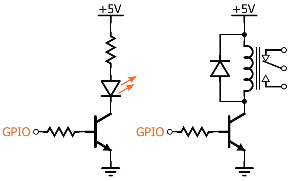
The proliferation of the Arduino, the Raspberry Pi, the TI MSP430 LaunchPad, and various other embedded development platforms has led to a corresponding proliferation of a basic switch/driver circuit based on an NPN bipolar junction transistor. This configuration allows a microcontroller output pin to safely and conveniently control high-current loads. The following diagram depicts two standard applications—high-intensity illumination with an LED and relay control.
This circuit certainly has its advantages:
- It’s simple and uses readily available parts.
- It’s flexible—a wide variety of voltages and load currents can be accommodated by choosing an appropriate transistor.
- You can easily migrate to a galvanically isolated implementation by using an optocoupler instead of a BJT.
However, it also comes with a risk: complacency. It’s simple and widespread, and this might encourage us to simply drop in a circuit that we find online and assume that it will work.
As is usually the case in life, one size doesn’t fit all. The following are important quantities that you need to consider before you finalize your BJT switch/driver design:
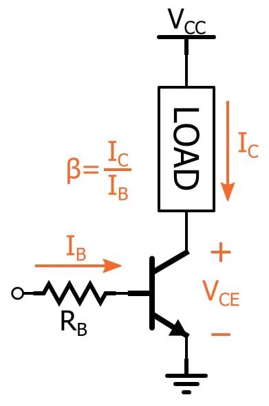
- BJT base current (IB), which is also the current sourced by the GPIO pin
- BJT active-region DC current gain (β)
- BJT collector current (IC), which is also the load current
Here is a visual representation:
IB should not exceed the maximum output current spec for the pin driving the base. To check this, assume a constant voltage drop of 0.7 V for the base-to-emitter junction. This gives you the following:
$$I_B=\frac{V_{IO}-0.7\ V}{R_B}$$
where VIO is the voltage supply for the chip’s input/output circuitry (common values are 5 V and 3.3 V).
Next we need to confirm that the collector current is 1) high enough to properly drive the load and 2) not so high that it causes the load to malfunction. The first step is to calculate an approximate minimum collector current using the BJT’s minimum value for active-region current gain.
$$ I_{Cmin}=I_B\times\beta_{min}$$
If this is less than your minimum acceptable load current, you cannot be certain that the circuit will function properly. To remedy this, increase the base current by using a smaller base resistor or choose a transistor with higher β.
The next step is to calculate the approximate maximum collector current using the maximum value for β. If ICmax is too high for your load, you need a resistor to limit the collector current. Whenever you force IC to be less than β × IB, you are moving the BJT into the saturation region—the additional voltage drop (created by the resistor) lowers the collector voltage and causes the base-to-collector junction to become insufficiently reverse-biased for active-region operation. (Actually, it is not practical to set the collector current using IC = β × IB because β is so variable; thus, you ensure that the transistor has more than enough current gain and then add resistance to limit IC). When you’re in saturation mode, you assume a fixed voltage for the collector-to-emitter junction, referred to as VCEsat; check the BJT’s datasheet, or use the common but imprecise value of 0.2 V. Then you use Ohm’s law in conjunction with VCC and VCEsat to calculate the collector current and confirm that it is in the acceptable range for your load.
Related Content