 Facebook
 Google
 GitHub
 Linkedin
Full-Adder
The half-adder is extremely useful until you want to add more than one binary digit quantities. The slow way to develop a two binary digit adders would be to make a truth table and reduce it. Then when you decide to make a three binary digit adder, do it again. Then when you decide to make a four digit adder, do it again. Then when ... The circuits would be fast, but development time would be slow.
Looking at a two binary digit sum shows what we need to extend addition to multiple binary digits.
           11
            11
            11
           ---
           110
Look at how many inputs the middle column uses. Our adder needs three inputs; a, b, and the carry from the previous sum, and we can use our two-input adder to build a three input adder.
Σ is the easy part. Normal arithmetic tells us that if Σ = a + b + Cin and Σ1 = a + b, then Σ = Σ1 + Cin.
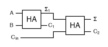
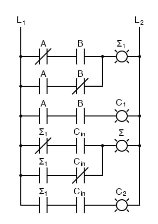
What do we do with C1 and C2? Let’s look at three input sums and quickly calculate:
Cin + a + b = ?
0 + 0 + 0 = 0       0 + 0 + 1 =  1       0 + 1 + 0 =  1      0 + 1 + 1 = 10
1 + 0 + 0 = 1       1 + 0 + 1 = 10       1 + 1 + 0 = 10      1 + 1 + 1 = 11
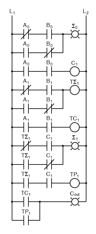
If you have any concern about the low order bit, please confirm that the circuit and ladder calculate it correctly.
In order to calculate the high order bit, notice that it is 1 in both cases when a + b produces a C1. Also, the high order bit is 1 when a + b produces a Σ1 and Cin is a 1. So We will have a carry when C1 OR (Σ1 AND Cin). Our complete three input adder is:
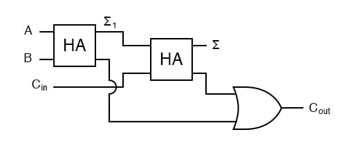
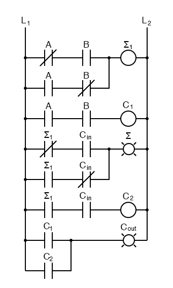
For some designs, being able to eliminate one or more types of gates can be important, and you can replace the final OR gate with an XOR gate without changing the results.
We can now connect two adders to add 2 bit quantities.
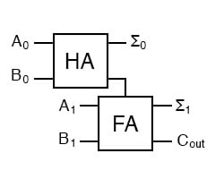
A0 is the low order bit of A, A1 is the high order bit of A, B0 is the low order bit of B, B1 is the high order bit of B, Σ0is the low order bit of the sum, Σ1 is the high order bit of the sum, and Cout is the Carry.
A two binary digit adder would never be made this way. Instead the lowest order bits would also go through a full adder.
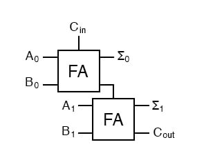
There are several reasons for this, one being that we can then allow a circuit to determine whether the lowest order carry should be included in the sum. This allows for the chaining of even larger sums. Consider two different ways to look at a four bit sum.
           111            1<-+  11<+-
            0110             |  01  |  10
            1011             |  10  |  11
           -----          -  | ---- | ---
           10001          1  +-100  +-101
If we allow the program to add a two bit number and remember the carry for later, then use that carry in the next sum the program can add any number of bits the user wants even though we have only provided a two-bit adder. Small PLCs can also be chained together for larger numbers.
These full adders can also can be expanded to any number of bits space allows. As an example, here’s how to do an 8 bit adder.
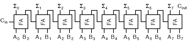
This is the same result as using the two 2-bit adders to make a 4-bit adder and then using two 4-bit adders to make an 8-bit adder or re-duplicating ladder logic and updating the numbers.
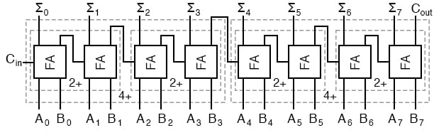
Each “2+” is a 2-bit adder and made of two full adders. Each “4+” is a 4-bit adder and made of two 2-bit adders. And the result of two 4-bit adders is the same 8-bit adder we used full adders to build.
For any large combinational circuit there are generally two approaches to design: you can take simpler circuits and replicate them; or you can design the complex circuit as a complete device. Using simpler circuits to build complex circuits allows a you to spend less time designing but then requires more time for signals to propagate through the transistors.
The 8-bit adder design above has to wait for all the Cxout signals to move from A0 + B0 up to the inputs of Σ7. If a designer builds an 8-bit adder as a complete device simplified to a sum of products, then each signal just travels through one NOT gate, one AND gate and one OR gate.
A seventeen input device has a truth table with 131,072 entries, and reducing 131,072 entries to a sum of products will take some time. When designing for systems that have a maximum allowed response time to provide the final result, you can begin by using simpler circuits and then attempt to replace portions of the circuit that are too slow.
That way you spend most of your time on the portions of a circuit that matter.
RELATED WORKSHEET:


