 Facebook
 Google
 GitHub
 Linkedin
Attenuators
What is Attenuators?
Attenuators are passive devices. It is convenient to discuss them along with decibels. Attenuators weaken or attenuate the high level output of a signal generator, for example, to provide a lower level signal for something like the antenna input of a sensitive radio receiver. (figure below) The attenuator could be built into the signal generator, or be a stand-alone device. It could provide a fixed or adjustable amount of attenuation. An attenuator section can also provide isolation between a source and a troublesome load.
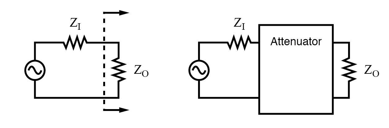
Constant impedance attenuator is matched to source impedance ZI and load impedance ZO. For radio frequency equipment Z is 50 Ω.
In the case of a stand-alone attenuator, it must be placed in series between the signal source and the load by breaking open the signal path as shown in the figure above. In addition, it must match both the source impedance ZI and the load impedance ZO, while providing a specified amount of attenuation. In this section we will only consider the special, and most common, case where the source and load impedances are equal. Not considered in this section, unequal source and load impedances may be matched by an attenuator section. However, the formulation is more complex.
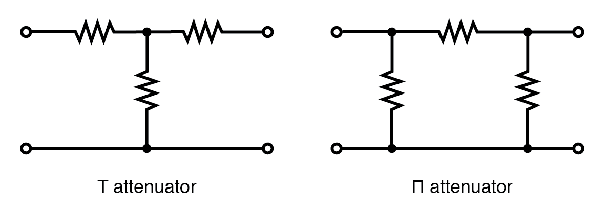
T section and Π section attenuators are common forms.
Common configurations are the T and Π networks shown in the figure above. Multiple attenuator sections may be cascaded when even weaker signals are needed as in the figure below.
Usage of Decibels for Attenuators
Voltage ratios, as used in the design of attenuators are often expressed in terms of decibels. The voltage ratio must be derived from the attenuation in decibels. Power ratios expressed as decibels are additive. For example, a 10 dB attenuator followed by a 6 dB attenuator provides 16dB of attenuation overall.
10 dB + 6 db = 16 dB
Changing sound levels are perceptible roughly proportional to the logarithm of the power ratio (PI / PO).
sound level = log10(PI / PO)
A change of 1 dB in sound level is barely perceptible to a listener, while 2 db is readily perceptible. An attenuation of 3dB corresponds to cutting power in half, while a gain of 3 db corresponds to a doubling of the power level. A gain of -3 dB is the same as an attenuation of +3 dB, corresponding to half the original power level.
The power change in decibels in terms of power ratio is:
dB = 10 log10(PI / PO)
Assuming that the load RI at PI is the same as the load resistor RO at PO(RI = RO), the decibels may be derived from the voltage ratio (VI / VO) or current ratio (II / IO):
PO = V O IO = VO2 / R = IO2 R PI = V I II = VI2 / R = II2 R dB = 10 log10(PI / PO) = 10 log10(VI2 / VO2) = 20 log10(VI/VO) dB = 10 log10(PI / PO) = 10 log10(II2 / IO2) = 20 log10(II/IO)
Decibel Equations
The two most often used forms of the decibel equation are:
dB = 10 log10(PI / PO) or dB = 20 log10(VI / VO)
We will use the latter form, since we need the voltage ratio. Once again, the voltage ratio form of equation is only applicable where the two corresponding resistors are equal. That is, the source and load resistance need to be equal.
Examples using the Decibel Equations
Example: Power into an attenuator is 10 Watts, the power out is 1 Watt. Find the attenuation in dB.
dB = 10 log10(PI / PO) = 10 log10 (10 /1) = 10 log10 (10) = 10 (1) = 10 dB
Example: Find the voltage attenuation ratio (K= (VI / VO)) for a 10 dB attenuator.
dB = 10= 20 log10(VI / VO) 10/20 = log10(VI / VO) 1010/20 = 10log10(VI / VO) 3.16 = (VI / VO) = AP(ratio)
Example: Power into an attenuator is 100 milliwatts, the power out is 1 milliwatt. Find the attenuation in dB.
dB = 10 log10(PI / PO) = 10 log10 (100 /1) = 10 log10 (100) = 10 (2) = 20 dB
Example: Find the voltage attenuation ratio (K= (VI / VO)) for a 20 dB attenuator.
dB = 20= 20 log10(VI / VO ) 1020/20 = 10 log10(VI / VO ) 10 = (VI / VO ) = K
T-section attenuator
The T and Π attenuators must be connected to a Z source and Z load impedance. The Z-(arrows) pointing away from the attenuator in the figure below indicate this. The Z-(arrows) pointing toward the attenuator indicates that the impedance seen looking into the attenuator with a load Z on the opposite end is Z, Z=50 Ω for our case. This impedance is a constant (50 Ω) with respect to attenuation– impedance does not change when attenuation is changed.
The table in the figure below lists resistor values for the T and Π attenuators to match a 50 Ω source/ load, as is the usual requirement in radio frequency work.
Telephone utility and other audio work often requires matching to 600 Ω. Multiply all R values by the ratio (600/50) to correct for 600 Ω matching. Multiplying by 75/50 would convert table values to match a 75 Ω source and load.
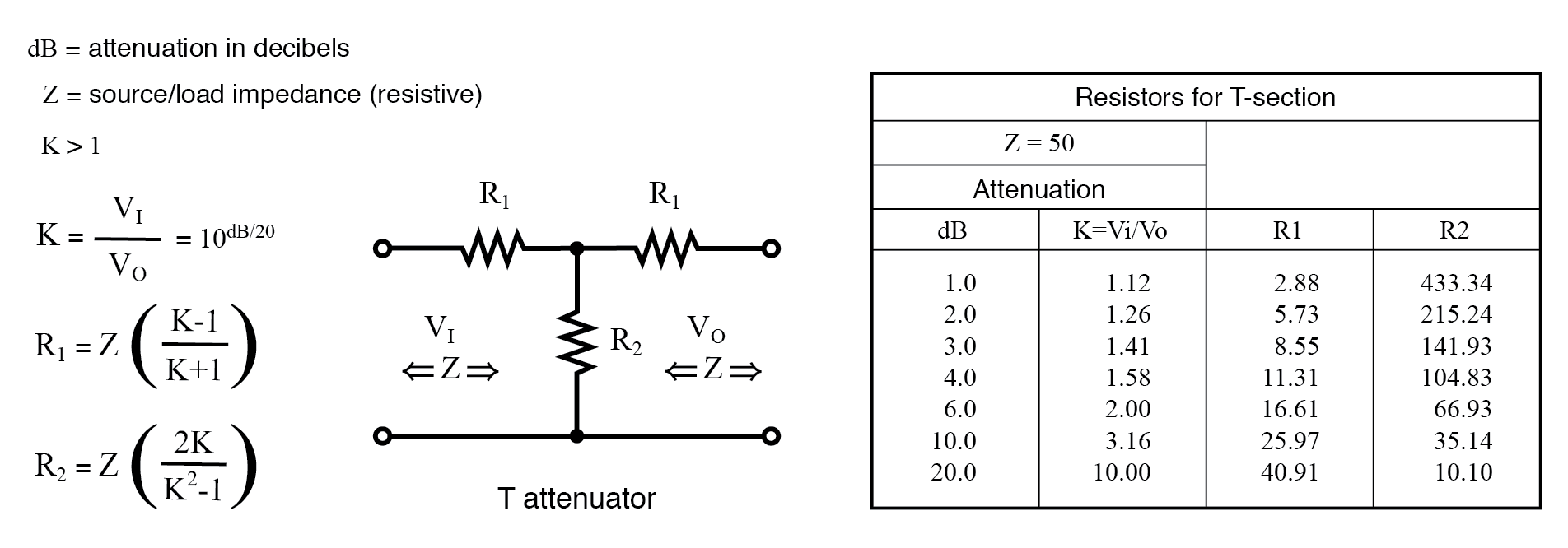
Formulas for T-section attenuator resistors, given K, the voltage attenuation ratio, and ZI = ZO = 50 Ω.
The amount of attenuation is customarily specified in dB (decibels). Though, we need the voltage (or current) ratio K to find the resistor values from equations. See the dB/20 term in the power of 10 term for computing the voltage ratio K from dB, above.
The T (and below Π) configurations are most commonly used as they provide bidirectional matching. That is, the attenuator input and output may be swapped end for end and still match the source and load impedances while supplying the same attenuation.
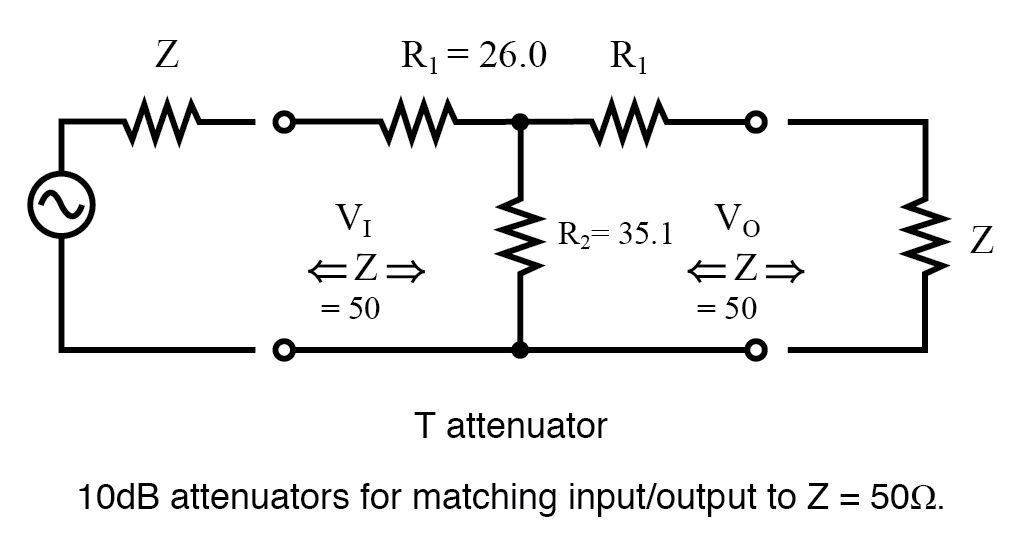
Disconnecting the source and looking in to the right at VI, we need to see a series parallel combination of R1, R2, R1, and Z looking like an equivalent resistance of ZIN, the same as the source/load impedance Z: (a load of Z is connected to the output.)
ZIN = R1 + (R2 ||(R1 + Z))
For example, substitute the 10 dB values from the 50 Ω attenuator table for R1 and R2 as shown in the figure below.
ZIN = 25.97 + (35.14 ||(25.97 + 50)) ZIN = 25.97 + (35.14 || 75.97 ) ZIN = 25.97 + 24.03 = 50
This shows us that we see 50 Ω looking right into the example attenuator (figure below) with a 50 Ω load.
Replacing the source generator, disconnecting load Z at VO, and looking in to the left, should give us the same equation as above for the impedance at VO, due to symmetry. Moreover, the three resistors must be values which supply the required attenuation from input to output. This is accomplished by the equations for R1 and R2 above as applied to the T-attenuator below.
PI-section attenuator
The table in the figure below lists resistor values for the Π attenuator matching a 50 Ω source/ load at some common attenuation levels. The resistors corresponding to other attenuation levels may be calculated from the equations.
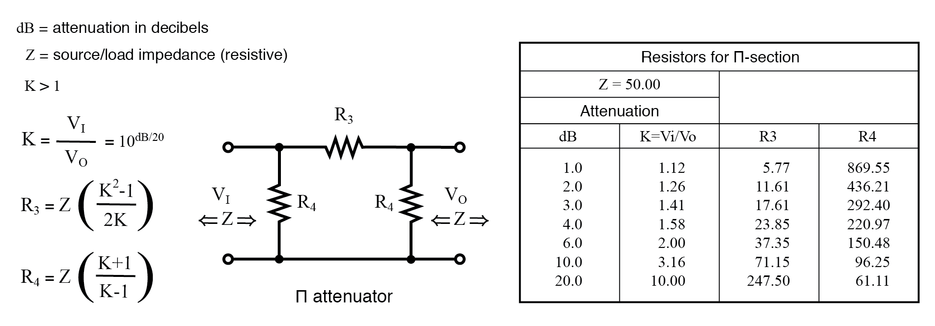
Formulas for Π-section attenuator resistors, given K, the voltage attenuation ratio, and ZI = ZO = 50 Ω.
The above apply to the π-attenuator below.
What resistor values would be required for both the Π attenuators for 10 dB of attenuation matching a 50 Ω source and load?
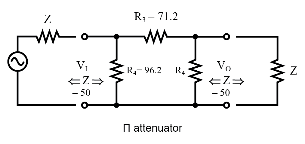
10 dB Π-section attenuator example for matching a 50 Ω source and load.
The 10 dB corresponds to a voltage attenuation ratio of K=3.16 in the next to last line of the above table. Transfer the resistor values in that line to the resistors on the schematic diagram in the figure above.
L-section attenuator
The table in the figure below lists resistor values for the L attenuators to match a 50 Ω source/ load. The table in the figure below also lists resistor values for an alternate form. Note that the resistor values are not the same.
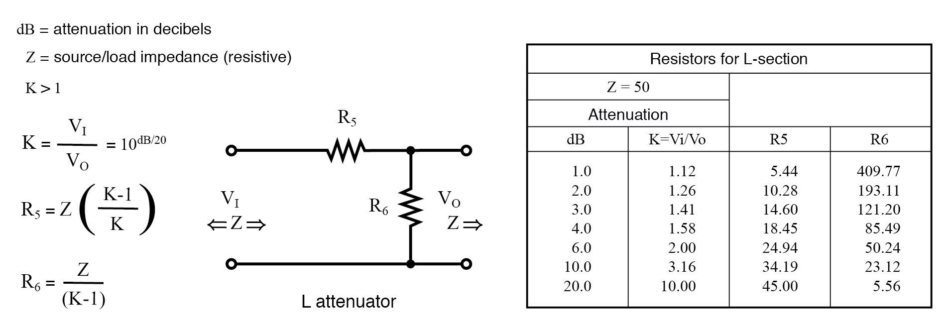
L-section attenuator table for 50 Ω source and load impedance.
The above apply to the L attenuator below.
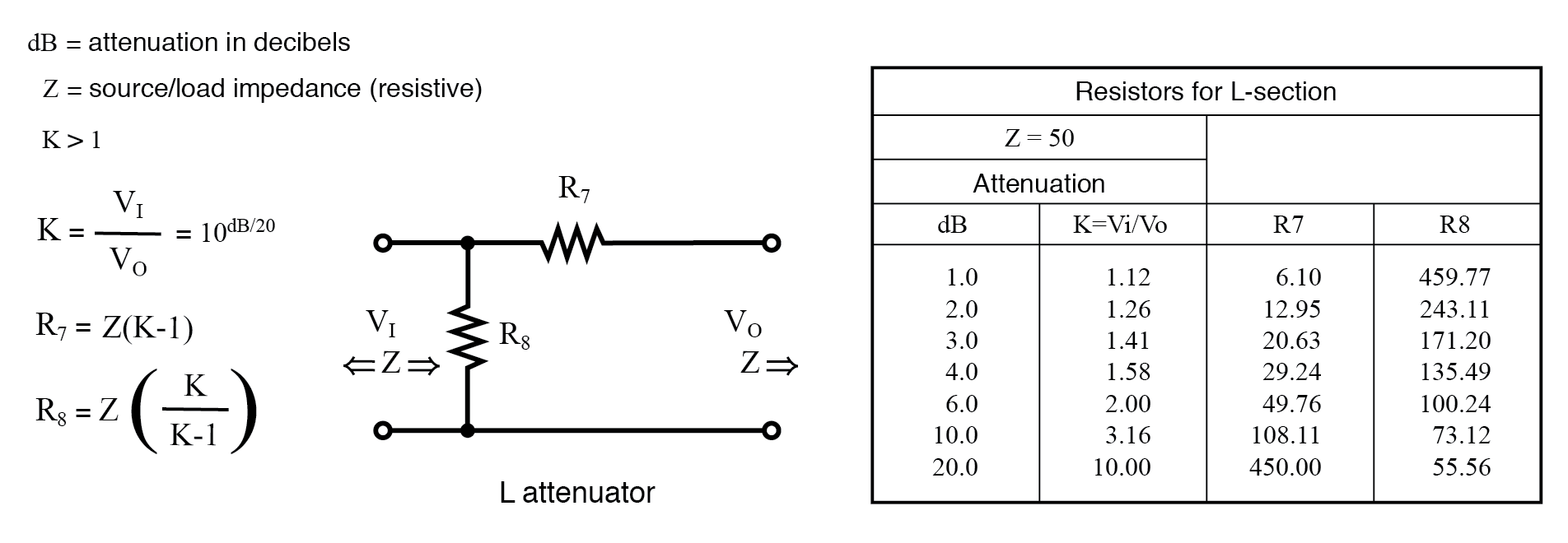
Alternate form L-section attenuator table for 50 Ω source and load impedance.
Bridged T attenuator
The table in the figure below lists resistor values for the bridged T attenuators to match a 50 Ω source and load. The bridged-T attenuator is not often used. Why not?
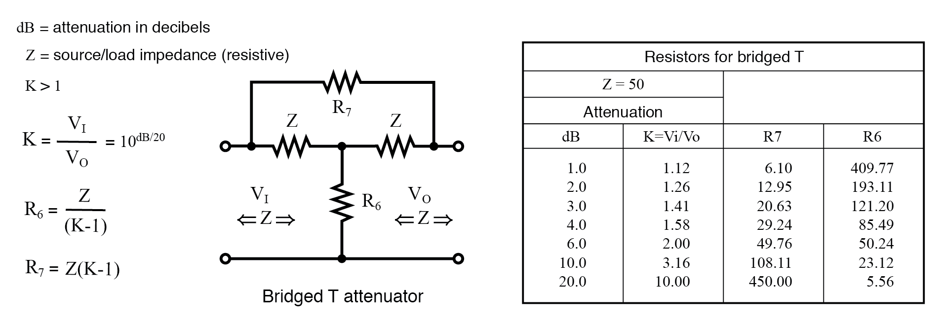
Formulas and abbreviated table for bridged-T attenuator section, Z = 50 Ω.
Cascaded sections
Attenuator sections can be cascaded as in the figure below for more attenuation than may be available from a single section. For example two 10 db attenuators may be cascaded to provide 20 dB of attenuation, the dB values being additive. The voltage attenuation ratio K or VI/VO for a 10 dB attenuator section is 3.16. The voltage attenuation ratio for the two cascaded sections is the product of the two Ks or 3.16x3.16=10 for the two cascaded sections.
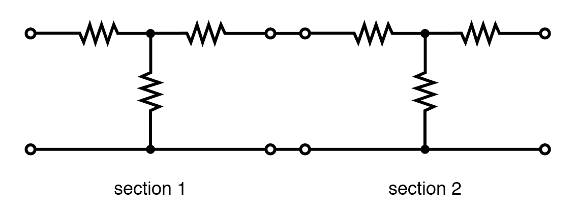
Cascaded attenuator sections: dB attenuation is additive.
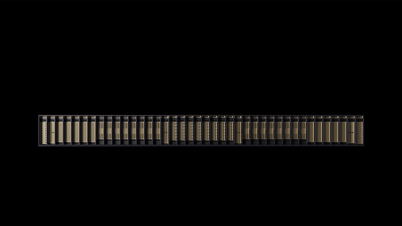
Variable attenuation can be provided in discrete steps by a switched attenuator. The example in the figure below, shown in the 0 dB position, is capable of 0 through 7 dB of attenuation by additive switching of none, one or more sections.
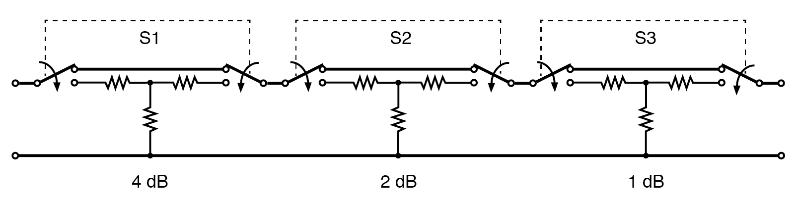
Switched attenuator: attenuation is variable in discrete steps.
The typical multi section attenuator has more sections than the above figure shows. The addition of a 3 or 8 dB section above enables the unit to cover to 10 dB and beyond. Lower signal levels are achieved by the addition of 10 dB and 20 dB sections, or a binary multiple 16 dB section.
RF attenuators
For radiofrequency (RF) work (<1000 Mhz), the individual sections must be mounted in shielded compartments to thwart capacitive coupling if lower signal levels are to be achieved at the highest frequencies. The individual sections of the switched attenuators in the previous section are mounted in shielded sections. Additional measures may be taken to extend the frequency range to beyond 1000 Mhz. This involves construction from special shaped lead-less resistive elements.
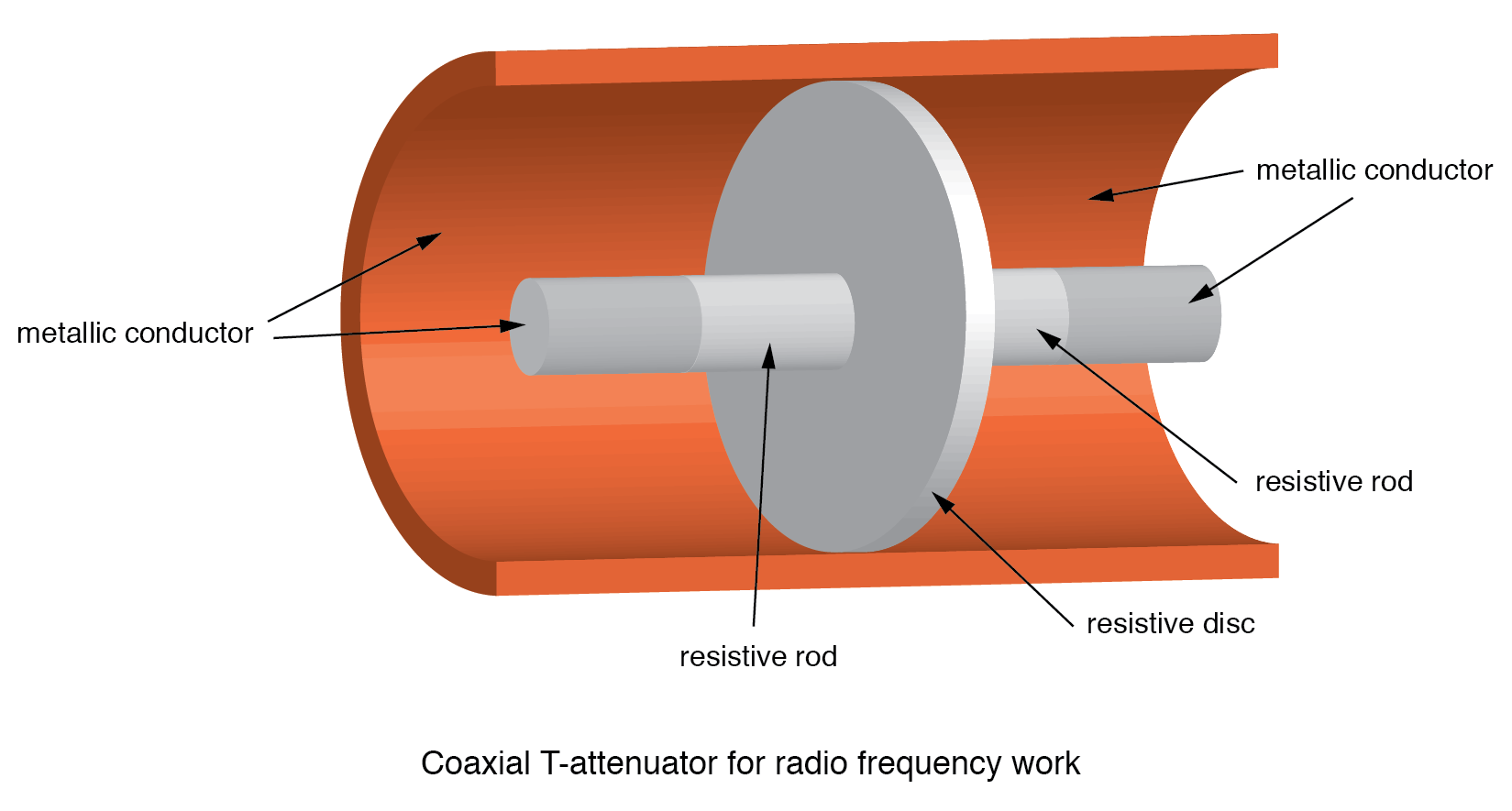
A coaxial T-section attenuator consisting of resistive rods and a resistive disk is shown in the figure above. This construction is usable to a few gigahertz. The coaxial Π version would have one resistive rod between two resistive disks in the coaxial line as in the figure below.
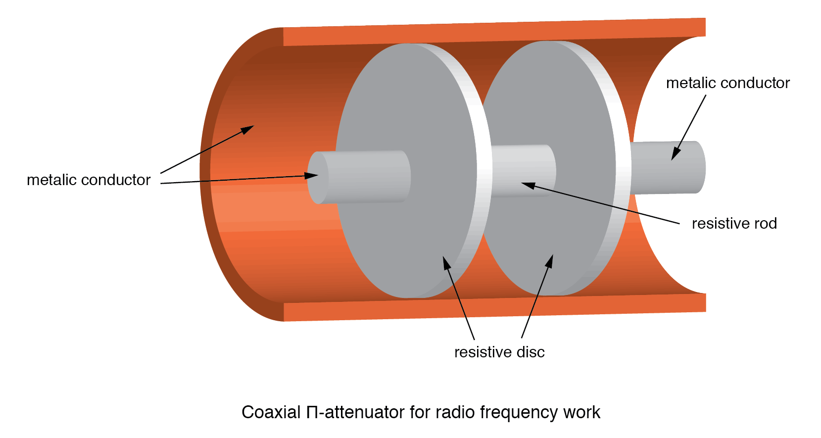
RF connectors, not shown, are attached to the ends of the above T and Π attenuators. The connectors allow individual attenuators to be cascaded, in addition to connecting between a source and load. For example, a 10 dB attenuator may be placed between a troublesome signal source and an expensive spectrum analyzer input. Even though we may not need the attenuation, the expensive test equipment is protected from the source by attenuating any overvoltage.
Summary: Attenuators
- An attenuator reduces an input signal to a lower level.
- The amount of attenuation is specified in decibels (dB). Decibel values are additive for cascaded attenuator sections.
- dB from power ratio: dB = 10 log10(PI / PO)
- dB from voltage ratio: dB = 20 log10(VI / VO)
- T and Π section attenuators are the most common circuit configurations.
RELATED WORKSHEETS:


When Was This Published? I need to Source It so I need a Publish date